Sand castle |
| 100 nF | SDA | SCL | V P= 5V to 8V |
| 100 nF |
pulse |
|
| |||||
|
|
|
| ||||
|
|
|
|
|
|
|
|
| 17 |
|
| 2 |
|
| 9 | 10 |
|
| 1 | 15 |
|
| SAND CASTLE PULSE | I2 C • BUS | Y delay |
| I2 C • BUS RECEIVERS |
|
|
|
| |||
|
| DETECTOR |
|
| V REF |
|
|
|
|
|
|
| V REF |
|
|
|
|
|
| Sand castle |
| Coring | Peaking |
| |||
|
|
|
|
|
|
| GENERATION | ||||||
|
|
| BK.H+V |
| DELAY TIME |
| 5V / 12V |
| on / off | frequency |
| ||
|
| BK |
|
|
|
|
|
|
|
|
| ||
|
|
|
| CONTROL |
|
|
|
|
|
|
| V REF | |
|
|
|
|
|
|
|
|
|
|
|
| ||
|
|
|
|
|
|
| V REF |
|
|
|
|
| |
|
|
|
|
|
|
|
|
|
|
| CORING |
| |
Y |
|
|
|
|
|
|
|
|
|
| 5 MHz |
| |
| BLACK LEVEL |
|
|
|
|
|
|
|
|
| |||
| 16 |
|
|
|
| 100 | 90 |
|
| ||||
| CLAMP |
|
|
|
|
| ns | ns |
|
|
| ||
100 nF |
|
|
|
|
|
|
| 2.6 MHz |
| ||||
|
|
|
|
|
|
|
|
|
|
|
| ||
|
|
|
|
|
|
|
|
|
|
|
|
| |
|
| V REF |
|
|
|
|
|
|
|
| CORING | ||
|
|
|
|
|
|
|
|
|
|
|
|
| 11 |
|
|
|
|
|
|
|
|
|
|
|
|
| 100 nF |
|
|
|
|
|
| Control signal |
|
|
| 5 MHz |
|
| |
|
|
|
|
|
|
|
|
|
|
|
| I2 C • BUS | |
|
|
|
|
|
|
|
|
|
|
|
| ||
|
|
|
|
|
|
|
|
|
|
| 2.6 MHz |
|
|
|
|
|
|
|
|
|
|
|
|
|
| PEAKING | |
|
|
|
|
|
|
|
|
|
|
|
|
| I2 C • BUS |
|
| 450 | 180 | BLACK | 180 | 90 | 45 | 90 | 100 | BLACK |
|
| |
|
| LEVEL | LEVEL | +1 |
| ||||||||
|
| ns | ns | ns | ns | ns | ns | ns |
| ||||
|
| CLAMP | CLAMP |
|
| ||||||||
|
|
|
|
|
|
|
|
|
|
| |||
100 nF |
| V REF |
|
|
|
|
|
|
|
|
|
|
|
| 13 |
|
|
|
|
|
|
|
|
|
| TDA4672 | Y |
100 nF |
|
|
|
|
|
|
|
|
|
|
| ||
14 |
|
|
|
|
|
|
|
|
|
| 12 | ||
|
|
|
|
|
|
|
|
|
|
|
|
| |
|
|
|
|
|
|
|
|
|
|
|
| ||
| 3 |
|
|
|
|
|
|
|
|
|
|
| 4 |
|
|
|
|
|
|
|
|
|
|
|
| ||
| 7 |
|
|
|
|
|
|
|
|
|
|
| 6 |
|
|
|
|
|
|
|
| 8 | 18 | 5 |
|
|
|
|
|
|
|
|
|
|
|
|
| NC |
|
| MED758 |
|
|
|
|
|
|
|
|
|
|
|
|
| |
|
|
|
|
| Fig. |
|
| ||||||
|
|
|
|
|
|
| FSW2 1 | 28 | SCL | ||||
|
|
|
|
|
|
|
|
|
| ||||
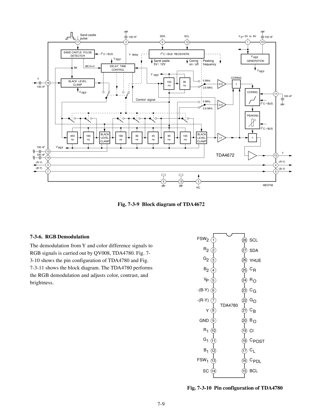
The demodulation from Y and color difference signals to RGB signals is carried out by QV008, TDA4780. Fig. 7-
R2 | 2 | 27 | SDA |
G2 | 3 | 26 | YHUE |
B2 | 4 | 25 | C R |
VP | 5 | 24 | R O |
6 | 23 | C G | |
7 | 22 | GO | |
|
| TDA4780 | C B |
Y | 8 | 21 | |
GND | 9 | 20 | B O |
R1 10 | 19 | Cl | |
G1 11 | 18 | C POST | |
B1 12 | 17 | C L | |
FSW1 13 | 16 | C PDL | |
SC 14 | 15 BCL |