ADSP-2181/ADSP-2183
•SPORTs support serial data word lengths from 3 to 16 bits and provide optional
•SPORT receive and transmit sections can generate unique in- terrupts on completing a data word transfer.
•SPORTs can receive and transmit an entire circular buffer of data with only one overhead cycle per data word. An interrupt is generated after a data buffer transfer.
•SPORT0 has a multichannel interface to selectively receive and transmit a 24 or 32 word,
•SPORT1 can be configured to have two external interrupts (IRQ0 and IRQ1) and the Flag In and Flag Out signals. The internally generated serial clock may still be used in this configuration.
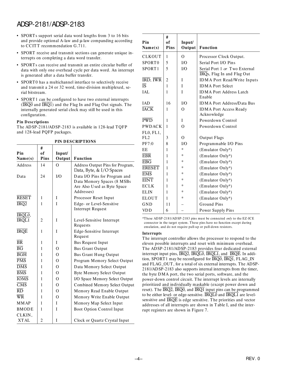
Pin Descriptions
The
PIN DESCRIPTIONS
|
|
|
|
|
|
|
|
|
|
|
|
|
|
| # |
|
|
Pin | of | Input/ |
| ||||||||||||||
Name(s) | Pins | Output | Function | ||||||||||||||
|
|
|
|
|
|
|
|
|
|
|
|
|
|
|
|
|
|
Address | 14 | O | Address Output Pins for Program, | ||||||||||||||
|
|
|
|
|
|
|
|
|
|
|
|
|
|
|
|
| Data, Byte, & I/O Spaces |
Data | 24 | I/O | Data I/O Pins for Program and | ||||||||||||||
|
|
|
|
|
|
|
|
|
|
|
|
|
|
|
|
| Data Memory Spaces (8 MSBs |
|
|
|
|
|
|
|
|
|
|
|
|
|
|
|
|
| Are Also Used as Byte Space |
|
|
|
|
|
|
|
|
|
|
|
|
|
|
|
|
| Addresses) |
|
|
|
|
|
|
|
|
|
|
|
|
|
|
| 1 | I | Processor Reset Input |
RESET | |||||||||||||||||
|
|
|
|
|
|
|
|
|
|
|
|
|
| 1 | I | Edge- or | |
IRQ2 | |||||||||||||||||
|
|
|
|
|
|
|
|
|
|
|
|
|
|
|
|
| Interrupt Request |
|
|
|
|
|
|
|
|
|
|
|
| , |
|
|
| ||
IRQL0 |
|
|
| ||||||||||||||
IRQL1 | 2 | I | |||||||||||||||
|
|
|
|
|
|
|
|
|
|
|
|
|
|
|
|
| Requests |
|
|
|
|
|
|
|
|
|
|
|
| 1 | I | ||||
IRQE | |||||||||||||||||
|
|
|
|
|
|
|
|
|
|
|
|
|
|
|
|
| Request |
|
|
|
|
|
|
|
|
|
|
| 1 | I | Bus Request Input | ||||
BR | |||||||||||||||||
|
|
|
|
|
|
|
|
|
| 1 | O | Bus Grant Output | |||||
BG | |||||||||||||||||
|
|
|
|
|
|
|
|
| 1 | O | Bus Grant Hung Output | ||||||
BGH | |||||||||||||||||
|
|
|
|
|
|
|
| 1 | O | Program Memory Select Output | |||||||
PMS | |||||||||||||||||
|
|
|
|
|
|
| 1 | O | Data Memory Select Output | ||||||||
DMS | |||||||||||||||||
|
|
|
|
|
| 1 | O | Byte Memory Select Output | |||||||||
BMS | |||||||||||||||||
|
|
|
|
| 1 | O | I/O Space Memory Select Output | ||||||||||
IOMS | |||||||||||||||||
|
|
|
| 1 | O | Combined Memory Select Output | |||||||||||
CMS | |||||||||||||||||
|
|
| 1 | O | Memory Read Enable Output | ||||||||||||
RD | |||||||||||||||||
|
| 1 | O | Memory Write Enable Output | |||||||||||||
WR | |||||||||||||||||
MMAP | 1 | I | Memory Map Select Input | ||||||||||||||
BMODE | 1 | I | Boot Option Control Input | ||||||||||||||
CLKIN, |
|
|
| ||||||||||||||
XTAL | 2 | I | Clock or Quartz Crystal Input | ||||||||||||||
|
|
|
|
|
|
|
|
|
|
|
|
|
|
|
|
|
|
|
|
|
|
|
|
|
|
|
|
|
| # |
|
|
|
|
Pin | of | Input/ |
|
|
| |||||||||||
Name(s) | Pins | Output | Function | |||||||||||||
|
|
|
|
|
|
|
|
|
|
|
|
|
|
|
|
|
CLKOUT | 1 | O | Processor Clock Output. | |||||||||||||
SPORT0 | 5 | I/O | Serial Port I/O Pins | |||||||||||||
SPORT1 | 5 | I/O | Serial Port 1 or Two External | |||||||||||||
|
|
|
|
|
|
|
|
|
|
|
|
|
|
| IRQ | s, Flag In and Flag Out |
|
| , |
|
|
|
|
|
|
| 2 | I |
| IDMA Port Read/Write Inputs | |||
IRD | IWR |
| ||||||||||||||
|
|
|
|
|
|
|
|
| 1 | I |
| IDMA Port Select | ||||
IS |
| |||||||||||||||
IAL | 1 | I | IDMA Port Address Latch | |||||||||||||
|
|
|
|
|
|
|
|
|
|
|
|
|
|
| Enable | |
IAD | 16 | I/O | IDMA Port Address/Data Bus | |||||||||||||
|
|
|
|
|
|
|
| 1 | O |
| IDMA Port Access Ready | |||||
IACK |
| |||||||||||||||
|
|
|
|
|
|
|
|
|
|
|
|
|
|
| Acknowledge | |
|
|
|
|
|
|
| 1 | I |
| Powerdown Control | ||||||
PWD |
| |||||||||||||||
PWDACK | 1 | O | Powerdown Control | |||||||||||||
FL0, FL1, |
|
|
|
|
| |||||||||||
FL2 | 3 | O |
| Output Flags | ||||||||||||
PF7:0 | 8 | I/O | Programmable I/O Pins | |||||||||||||
EE | 1 | * | (Emulator Only*) | |||||||||||||
|
|
|
|
|
| 1 | * |
| (Emulator Only*) | |||||||
EBR |
| |||||||||||||||
|
|
|
|
| 1 | * |
| (Emulator Only*) | ||||||||
EBG |
| |||||||||||||||
|
|
|
| 1 | * |
| (Emulator Only*) | |||||||||
ERESET |
| |||||||||||||||
|
|
| 1 | * |
| (Emulator Only*) | ||||||||||
EMS |
| |||||||||||||||
|
| 1 | * |
| (Emulator Only*) | |||||||||||
EINT |
| |||||||||||||||
ECLK | 1 | * | (Emulator Only*) | |||||||||||||
ELIN | 1 | * | (Emulator Only*) | |||||||||||||
ELOUT | 1 | * | (Emulator Only*) | |||||||||||||
GND | 11 | – | Ground Pins | |||||||||||||
VDD | 6 | – | Power Supply Pins | |||||||||||||
|
|
|
|
|
|
|
|
|
|
|
|
|
|
|
|
|
*These
Interrupts
The interrupt controller allows the processor to respond to the eleven possible interrupts and reset with minimum overhead. The
REV. 0 |