Analog Devices ADSP-2181, ADSP-2183 manual Booting Method, Idma Port Booting

Models: ADSP-2183 ADSP-2181

1 40
Download 40 pages 6.22 Kb
Page 9
Image 9

ADSP-2181/ADSP-2183

When the BWCOUNT register is written with a nonzero value the BDMA circuit starts executing byte memory accesses with wait states set by BMWAIT. These accesses continue until the count reaches zero. When enough accesses have occurred to create a destination word, it is transferred to or from on-chip memory. The transfer takes one DSP cycle. DSP accesses to ex- ternal memory have priority over BDMA byte memory accesses.

The BDMA Context Reset bit (BCR) controls whether the processor is held off while the BDMA accesses are occurring. Setting the BCR bit to 0 allows the processor to continue opera- tions. Setting the BCR bit to 1 causes the processor to stop ex- ecution while the BDMA accesses are occurring, to clear the context of the processor, and start execution at address 0 when the BDMA accesses have completed.

Internal Memory DMA Port (IDMA Port)

The IDMA Port provides an efficient means of communication between a host system and the ADSP-2181/ADSP-2183. The port is used to access the on-chip program memory and data memory of the DSP with only one DSP cycle per word over- head. The IDMA port cannot be used, however, to write to the DSP’s memory-mapped control registers.

The IDMA port has a 16-bit multiplexed address and data bus and supports 24-bit program memory. The IDMA port is com- pletely asynchronous and can be written to while the ADSP- 2181/ADSP-2183 is operating at full speed.

The DSP memory address is latched and then is automatically incremented after each IDMA transaction. An external device can therefore access a block of sequentially addressed memory by specifying only the starting address of the block. This in- creases throughput as the address does not have to be sent for each memory access.

IDMA Port access occurs in two phases. The first is the IDMA Address Latch cycle. When the acknowledge is asserted, a 14- bit address and 1-bit destination type can be driven onto the bus by an external device. The address specifies an on-chip memory location, the destination type specifies whether it is a DM or PM access. The falling edge of the address latch signal latches this value into the IDMAA register.

Once the address is stored, data can then be either read from, or written to, the ADSP-2181/ADSP-2183’s on-chip memory. As- serting the select line (IS) and the appropriate read or write line (IRD and IWR respectively) signals the ADSP-2181/ADSP- 2183 that a particular transaction is required. In either case, there is a one-processor-cycle delay for synchronization. The memory access consumes one additional processor cycle.

Once an access has occurred, the latched address is automati- cally incremented, and another access can occur.

Through the IDMAA register, the DSP can also specify the starting address and data format for DMA operation.

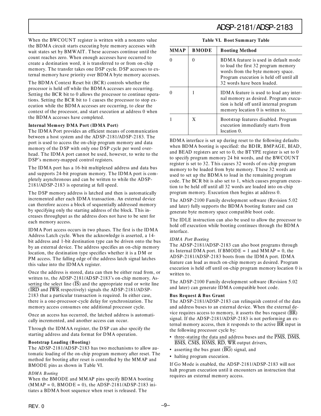
Table VI. Boot Summary Table

MMAP

BMODE

Booting Method


0

0

BDMA feature is used in default mode


to load the first 32 program memory


words from the byte memory space.


Program execution is held off until all


32 words have been loaded.


0

1

IDMA feature is used to load any inter-


nal memory as desired. Program execu-


tion is held off until internal program


memory location 0 is written to.


1

X

Bootstrap features disabled. Program


execution immediately starts from


location 0.


BDMA interface is set up during reset to the following defaults when BDMA booting is specified: the BDIR, BMPAGE, BIAD, and BEAD registers are set to 0, the BTYPE register is set to 0 to specify program memory 24 bit words, and the BWCOUNT register is set to 32. This causes 32 words of on-chip program memory to be loaded from byte memory. These 32 words are used to set up the BDMA to load in the remaining program code. The BCR bit is also set to 1, which causes program execu- tion to be held off until all 32 words are loaded into on-chip program memory. Execution then begins at address 0.

The ADSP-2100 Family development software (Revision 5.02 and later) fully supports the BDMA booting feature and can generate byte memory space compatible boot code.

The IDLE instruction can also be used to allow the processor to hold off execution while booting continues through the BDMA interface.

IDMA Port Booting

The ADSP-2181/ADSP-2183 can also boot programs through its Internal DMA port. If BMODE = 1 and MMAP = 0, the ADSP-2181/ADSP-2183 boots from the IDMA port. IDMA feature can load as much on-chip memory as desired. Program execution is held off until on-chip program memory location 0 is written to.

The ADSP-2100 Family development software (Revision 5.02 and later) can generate IDMA compatible boot code.

Bus Request & Bus Grant

The ADSP-2181/ADSP-2183 can relinquish control of the data and address buses to an external device. When the external de- vice requires access to memory, it asserts the bus request (BR) signal. If the ADSP-2181/ADSP-2183 is not performing an ex- ternal memory access, then it responds to the active BR input in the following processor cycle by:

three-stating the data and address buses and the PMS, DMS,

Bootstrap Loading (Booting)

The ADSP-2181/ADSP-2183 has two mechanisms to allow au- tomatic loading of the on-chip program memory after reset. The method for booting after reset is controlled by the MMAP and BMODE pins as shown in Table VI.

BDMA Booting

When the BMODE and MMAP pins specify BDMA booting (MMAP = 0, BMODE = 0), the ADSP-2181/ADSP-2183 ini- tiates a BDMA boot sequence when reset is released. The

REV. 0

BMS, CMS, IOMS, RD, WR output drivers,

asserting the bus grant (BG) signal, and

halting program execution.

If Go Mode is enabled, the ADSP-2181/ADSP-2183 will not halt program execution until it encounters an instruction that requires an external memory access.

–9–

Page 9
Image 9
Analog Devices ADSP-2181, ADSP-2183 manual Booting Method, Idma Port Booting