ADSP-2181/ADSP-2183
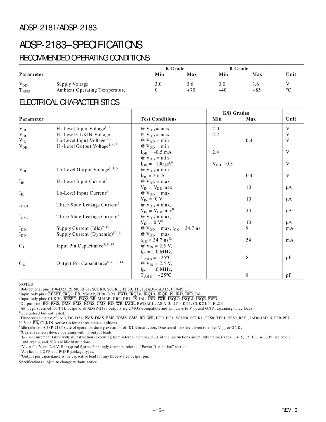
ADSP-2183–SPECIFICATIONS
RECOMMENDED OPERATING CONDITIONS
|
|
| K Grade |
| B Grade |
|
Parameter |
| Min | Max | Min | Max | Unit |
|
|
|
|
|
|
|
VDD | Supply Voltage | 3.0 | 3.6 | 3.0 | 3.6 | V |
TAMB | Ambient Operating Temperature | 0 | +70 | +85 | °C |
ELECTRICAL CHARACTERISTICS
|
|
|
| K/B Grades |
|
Parameter |
| Test Conditions | Min | Max | Unit |
|
|
|
|
|
|
VIH | @ VDD = max | 2.0 |
| V | |
VIH | @ VDD = max | 2.2 |
| V | |
VIL | @ VDD = min |
| 0.4 | V | |
VOH | @ VDD = min |
|
|
| |
|
| IOH = | 2.4 |
| V |
|
| @ VDD = min |
|
|
|
VOL | IOH = | VDD – 0.3 | V | ||
@ VDD = min |
|
|
| ||
IIH | IOL = 2 mA |
| 0.4 | V | |
@ VDD = max |
|
| μA | ||
IIL | VIN = VDD max |
| 10 | ||
@ VDD = max |
|
| μA | ||
IOZH | VIN = 0 V |
| 10 | ||
@ VDD = max, |
|
| μA | ||
IOZL | VIN = VDD max8 |
| 10 | ||
@ VDD = max, |
|
| μA | ||
IDD | Supply Current (Idle)9, 10 | VIN = 0 V8 |
| 10 | |
@ VDD = max, tCK = 34.7 ns |
| 9 | mA | ||
IDD | Supply Current (Dynamic)10, 11 | @ VDD = max |
|
|
|
CI | Input Pin Capacitance3, 6, 13 | tCK = 34.7 ns12 |
| 54 | mA |
@ VIN = 2.5 V, |
|
|
| ||
|
| fIN = 1.0 MHz, |
|
|
|
CO | Output Pin Capacitance6, 7, 13, 14 | TAMB = +25°C |
| 8 | pF |
@ VIN = 2.5 V, |
|
|
| ||
|
| fIN = 1.0 MHz, |
|
|
|
|
| TAMB = +25°C |
| 8 | pF |
NOTES
1Bidirectional pins:
2Input only pins: RESET, IRQ2, BR, MMAP, DR0, DR1, PWD, IRQL0, IRQL1, IRQE, IS, IRD, IWR, IAL.
3Input only pins: CLKIN, RESET, IRQ2, BR, MMAP, DR0, DR1, IS, IAL, IRD, IWR, IRQL0, IRQL1, IRQE, PWD.
4Output pins: BG, PMS, DMS, BMS, IOMS, CMS, RD, WR, IACK, PWDACK,
5Although specified for TTL outputs, all
80 V on BR, CLKIN Active (to force
9Idle refers to
10Current reflects device operating with no output loads.
11IDD measurement taken with all instructions executing from internal memory. 50% of the instructions are multifunction (types 1, 4, 5, 12, 13, 14), 30% are type 2 and type 6, and 20% are idle instructions.
12VIN = 0.4 V and 2.4 V. For typical figures for supply currents, refer to “Power Dissipation” section.
13Applies to TQFP and PQFP package types.
14Output pin capacitance is the capacitive load for any
Specifications subject to change without notice.
REV. 0 |