ADSP-2181
CAPACITIVE LOADING
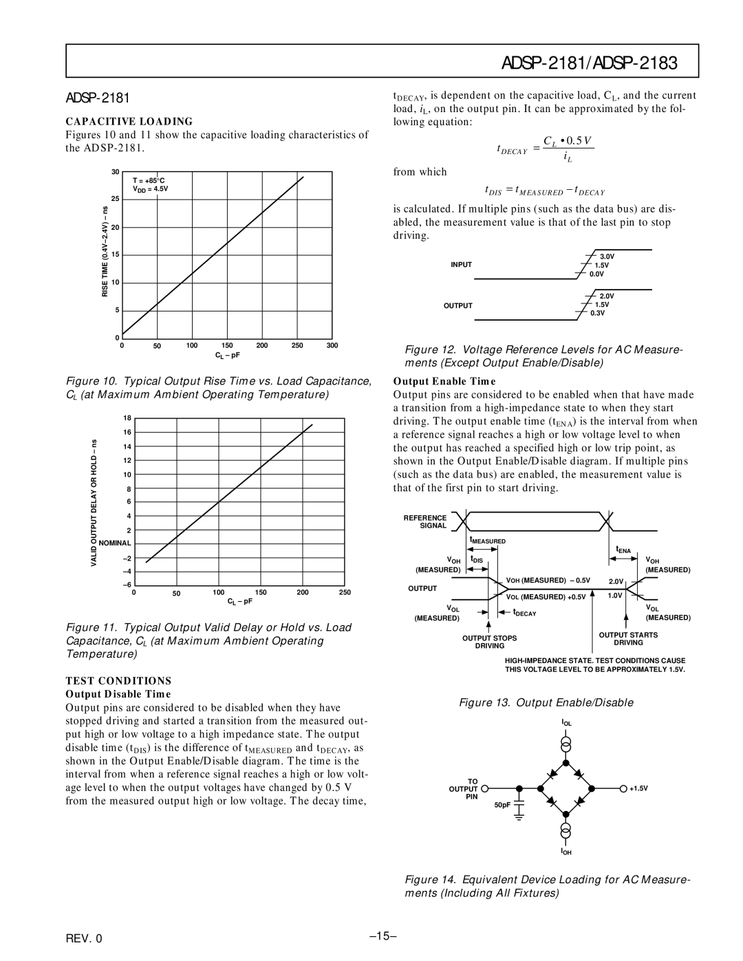
Figures 10 and 11 show the capacitive loading characteristics of the ADSP-2181.
| 30 |
|
|
|
|
|
|
|
|
|
|
|
|
|
|
|
|
|
|
|
|
|
|
|
|
|
|
| |
|
|
| T = +85 | °C |
|
|
|
|
|
|
|
|
|
|
|
|
| VDD = 4.5V |
|
|
|
|
|
|
|
|
|
| |
– ns | 25 |
|
|
|
|
|
|
|
|
|
|
|
|
|
|
|
|
|
|
|
|
|
|
|
|
|
| ||
|
|
|
|
|
|
|
|
|
|
|
|
|
| |
2.4V) | 20 |
|
|
|
|
|
|
|
|
|
|
|
|
|
15 |
|
|
|
|
|
|
|
|
|
|
|
|
| |
|
|
|
|
|
|
|
|
|
|
|
|
|
| |
RISE | 10 |
|
|
|
|
|
|
|
|
|
|
|
|
|
|
|
|
|
|
|
|
|
|
|
|
|
| ||
|
|
|
|
|
|
|
|
|
|
|
|
|
| |
| 5 |
|
|
|
|
|
|
|
|
|
|
|
|
|
|
|
|
|
|
|
|
|
|
|
|
|
|
| |
| 0 |
|
|
|
|
|
|
|
|
|
|
|
|
|
| 0 | 50 | 100 | 150 | 200 | 250 | 300 | |||||||
|
|
|
|
|
|
| CL – pF |
|
|
|
|
|
| |
Figure 10. Typical Output Rise Time vs. Load Capacitance, CL (at Maximum Ambient Operating Temperature)
| 18 | |
| 16 | |
ns | 14 | |
– | ||
| ||
HOLD | 12 | |
10 | ||
OR | ||
8 | ||
DELAY | ||
6 | ||
|
ADSP-2181/ADSP-2183
tDECAY, is dependent on the capacitive load, CL, and the current load, iL, on the output pin. It can be approximated by the fol-
lowing equation:
tDECAY = CL •i0.5V L
from which
tDIS = tMEASURED – tDECAY
is calculated. If multiple pins (such as the data bus) are dis- abled, the measurement value is that of the last pin to stop driving.
3.0V
INPUT1.5V 0.0V
2.0V
OUTPUT1.5V 0.3V
Figure 12. Voltage Reference Levels for AC Measure- ments (Except Output Enable/Disable)
Output Enable Time
Output pins are considered to be enabled when that have made a transition from a
OUTPUT | 4 | |
2 | ||
NOMINAL | ||
VALID | ||
| ||
|
0 | 50 | 100 | 150 | 200 | 250 |
CL – pF
Figure 11. Typical Output Valid Delay or Hold vs. Load Capacitance, CL (at Maximum Ambient Operating Temperature)
REFERENCE
SIGNAL
tMEASURED
VOH tDIS
(MEASURED)
VOH (MEASURED) – 0.5V
OUTPUT
VOL (MEASURED) +0.5V
VOL |
|
|
| tDECAY |
(MEASURED) |
| |||
|
| |||
OUTPUT STOPS
DRIVING
tENA
VOH
(MEASURED)
2.0V
1.0V
VOL
(MEASURED)
OUTPUT STARTS
DRIVING
TEST CONDITIONS
Output Disable Time
Output pins are considered to be disabled when they have stopped driving and started a transition from the measured out- put high or low voltage to a high impedance state. The output
disable time (tDIS) is the difference of tMEASURED and tDECAY, as shown in the Output Enable/Disable diagram. The time is the
interval from when a reference signal reaches a high or low volt- age level to when the output voltages have changed by 0.5 V from the measured output high or low voltage. The decay time,
THIS VOLTAGE LEVEL TO BE APPROXIMATELY 1.5V.
Figure 13. Output Enable/Disable
IOL
TO
OUTPUT ![]()
![]()
![]()
![]()
![]() +1.5V PIN
+1.5V PIN
50pF
IOH
Figure 14. Equivalent Device Loading for AC Measure- ments (Including All Fixtures)
REV. 0 |