Analog Devices manual ADSP-2181/ADSP-2183, Architecture Overview

Models: ADSP-2183 ADSP-2181

1 40
Download 40 pages 6.22 Kb
Page 2
Image 2

ADSP-2181/ADSP-2183

This takes place while the processor continues to:

receive and transmit data through the two serial ports

receive and/or transmit data through the internal DMA port

receive and/or transmit data through the byte DMA port

decrement timer

Development System

The ADSP-2100 Family Development Software, a complete set of tools for software and hardware system development, supports the ADSP-2181/ADSP-2183. The System Builder provides a high level method for defining the architecture of systems under devel- opment. The Assembler has an algebraic syntax that is easy to program and debug. The Linker combines object files into an executable file. The Simulator provides an interactive instruc- tion-level simulation with a reconfigurable user interface to dis- play different portions of the hardware environment. A PROM Splitter generates PROM programmer compatible files. The C Compiler, based on the Free Software Foundation’s GNU C Compiler, generates ADSP-2181/ADSP-2183 assembly source code. The source code debugger allows programs to be corrected in the C environment. The Runtime Library includes over 100 ANSI-standard mathematical and DSP-specific functions.

The EZ-KIT Lite is a hardware/software kit offering a complete development environment for the entire ADSP-21xx family: an ADSP-2181 based evaluation board with PC monitor software plus Assembler, Linker, Simulator, and PROM Splitter software. The ADSP-2181 EZ-KIT Lite is a low cost, easy to use hardware platform on which you can quickly get started with your DSP soft- ware design. The EZ-KIT Lite includes the following features:

33 MHz ADSP-2181

Full 16-bit Stereo Audio I/O with AD1847 SoundPort®Codec

RS-232 Interface to PC with Windows 3.1 Control Software

Stand-Alone Operation with Socketed EPROM

EZ-ICE Connector for Emulator Control

DSP Demo Programs

The ADSP-2181 EZ-ICE®Emulator aids in the hardware de- bugging of ADSP-2181 system. The emulator consists of hard- ware, host computer resident software, and the target board connector. The ADSP-2181/ADSP-2183 integrates on-chip emulation support with a 14-pin ICE-Port interface. This inter- face provides a simpler target board connection that requires fewer mechanical clearance considerations than other ADSP-2100 Family EZ-ICEs. The ADSP-2181/ADSP-2183 device need not be removed from the target system when using the EZ-ICE, nor are any adapters needed. Due to the small footprint of the EZ-ICE connector, emulation can be supported in final board designs.

The EZ-ICE performs a full range of functions, including:

Stand-alone or in-target operation

Up to 20 breakpoints

Single-step or full-speed operation

Registers and memory values can be examined and altered

PC upload and download functions

Instruction-level emulation of program booting and execution

Complete assembly and disassembly of instructions

C source-level debugging

See “Designing An EZ-ICE-Compatible Target System” in the ADSP-2100 Family EZ-Tools Manual as well as page 11 of this data sheet for exact specifications of the EZ-ICE target board connector.

EZ-ICE and SoundPort are registered trademarks of Analog Devices, Inc.

Additional Information

This data sheet provides a general overview of ADSP-2181/ ADSP-2183 functionality. For additional information on the architecture and instruction set of the processor, refer to the ADSP-2100 Family User’s Manual. For more information about the development tools, refer to the ADSP-2100 Family Develop- ment Tools Data Sheet.

ARCHITECTURE OVERVIEW

The ADSP-2181/ADSP-2183 instruction set provides flexible data moves and multifunction (one or two data moves with a computation) instructions. Every instruction can be executed in

asingle processor cycle. The ADSP-2181/ADSP-2183 assembly language uses an algebraic syntax for ease of coding and read- ability. A comprehensive set of development tools supports pro- gram development.

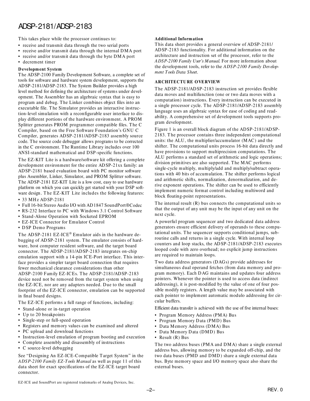
Figure 1 is an overall block diagram of the ADSP-2181/ADSP- 2183. The processor contains three independent computational units: the ALU, the multiplier/accumulator (MAC) and the shifter. The computational units process 16-bit data directly and have provisions to support multiprecision computations. The ALU performs a standard set of arithmetic and logic operations; division primitives are also supported. The MAC performs single-cycle multiply, multiply/add and multiply/subtract opera- tions with 40 bits of accumulation. The shifter performs logical and arithmetic shifts, normalization, denormalization, and de- rive exponent operations. The shifter can be used to efficiently implement numeric format control including multiword and block floating-point representations.

The internal result (R) bus connects the computational units so that the output of any unit may be the input of any unit on the next cycle.

A powerful program sequencer and two dedicated data address generators ensure efficient delivery of operands to these compu- tational units. The sequencer supports conditional jumps, sub- routine calls and returns in a single cycle. With internal loop counters and loop stacks, the ADSP-2181/ADSP-2183 executes looped code with zero overhead; no explicit jump instructions are required to maintain loops.

Two data address generators (DAGs) provide addresses for simultaneous dual operand fetches (from data memory and pro- gram memory). Each DAG maintains and updates four address pointers. Whenever the pointer is used to access data (indirect addressing), it is post-modified by the value of one of four pos- sible modify registers. A length value may be associated with each pointer to implement automatic modulo addressing for cir- cular buffers.

Efficient data transfer is achieved with the use of five internal buses:

Program Memory Address (PMA) Bus

Program Memory Data (PMD) Bus

Data Memory Address (DMA) Bus

Data Memory Data (DMD) Bus

Result (R) Bus

The two address buses (PMA and DMA) share a single external address bus, allowing memory to be expanded off-chip, and the two data buses (PMD and DMD) share a single external data bus. Byte memory space and I/O memory space also share the external buses.

–2–

REV. 0

Page 2
Image 2
Analog Devices manual ADSP-2181/ADSP-2183, Architecture Overview