ADSP-2181/ADSP-2183
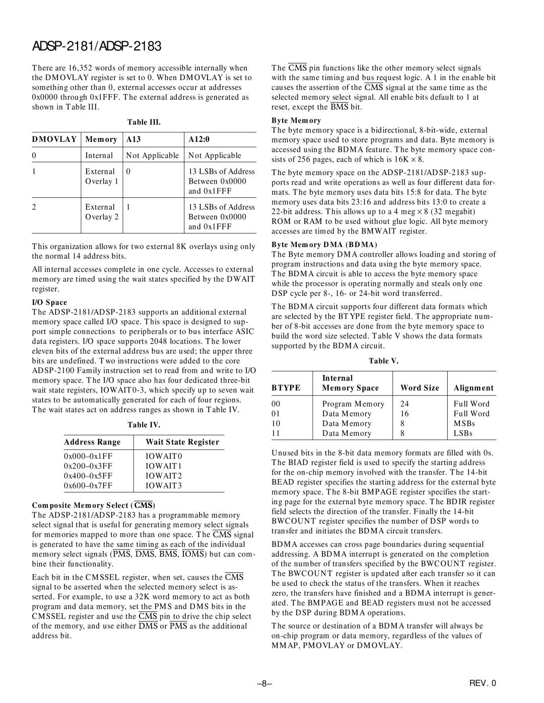
There are 16,352 words of memory accessible internally when the DMOVLAY register is set to 0. When DMOVLAY is set to something other than 0, external accesses occur at addresses 0x0000 through 0x1FFF. The external address is generated as shown in Table III.
Table III.
DMOVLAY | Memory | A13 | A12:0 |
|
|
|
|
0 | Internal | Not Applicable | Not Applicable |
|
|
|
|
1 | External | 0 | 13 LSBs of Address |
| Overlay 1 |
| Between 0x0000 |
|
|
| and 0x1FFF |
|
|
|
|
2 | External | 1 | 13 LSBs of Address |
| Overlay 2 |
| Between 0x0000 |
|
|
| and 0x1FFF |
|
|
|
|
This organization allows for two external 8K overlays using only the normal 14 address bits.
All internal accesses complete in one cycle. Accesses to external memory are timed using the wait states specified by the DWAIT register.
I/O Space
The
| Table IV. | |
|
|
|
Address Range |
| Wait State Register |
|
|
|
| IOWAIT0 | |
| IOWAIT1 | |
| IOWAIT2 | |
| IOWAIT3 | |
|
|
|
Composite Memory Select (CMS)
The
Each bit in the CMSSEL register, when set, causes the CMS signal to be asserted when the selected memory select is as- serted. For example, to use a 32K word memory to act as both program and data memory, set the PMS and DMS bits in the CMSSEL register and use the CMS pin to drive the chip select of the memory, and use either DMS or PMS as the additional address bit.
The CMS pin functions like the other memory select signals with the same timing and bus request logic. A 1 in the enable bit causes the assertion of the CMS signal at the same time as the selected memory select signal. All enable bits default to 1 at reset, except the BMS bit.
Byte Memory
The byte memory space is a bidirectional,
The byte memory space on the
Byte Memory DMA (BDMA)
The Byte memory DMA controller allows loading and storing of program instructions and data using the byte memory space. The BDMA circuit is able to access the byte memory space while the processor is operating normally and steals only one DSP cycle per
The BDMA circuit supports four different data formats which are selected by the BTYPE register field. The appropriate num- ber of
Table V.
| Internal |
|
|
BTYPE | Memory Space | Word Size | Alignment |
|
|
|
|
00 | Program Memory | 24 | Full Word |
01 | Data Memory | 16 | Full Word |
10 | Data Memory | 8 | MSBs |
11 | Data Memory | 8 | LSBs |
|
|
|
|
Unused bits in the
BDMA accesses can cross page boundaries during sequential addressing. A BDMA interrupt is generated on the completion of the number of transfers specified by the BWCOUNT register. The BWCOUNT register is updated after each transfer so it can be used to check the status of the transfers. When it reaches zero, the transfers have finished and a BDMA interrupt is gener- ated. The BMPAGE and BEAD registers must not be accessed by the DSP during BDMA operations.
The source or destination of a BDMA transfer will always be
REV. 0 |