ADSP-2181/ADSP-2183
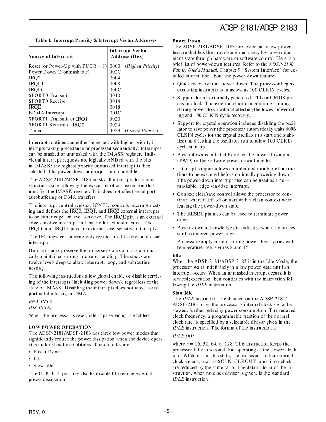
Table I. Interrupt Priority & Interrupt Vector Addresses
|
|
|
|
|
|
|
| Interrupt Vector | |
Source of Interrupt | Address (Hex) | ||||||||
|
|
|
|
|
|
|
|
|
|
Reset (or | 0000 | (Highest Priority) | |||||||
Power Down (Nonmaskable) | 002C |
| |||||||
IRQ2 | 0004 |
| |||||||
IRQL1 |
|
|
|
|
|
| 0008 |
| |
IRQL0 |
|
|
|
|
| 000C |
| ||
SPORT0 Transmit | 0010 |
| |||||||
SPORT0 Receive | 0014 |
| |||||||
IRQE |
|
|
|
|
| 0018 |
| ||
BDMA Interrupt | 001C |
| |||||||
SPORT1 Transmit or | IRQ1 |
| 0020 |
| |||||
SPORT1 Receive or | IRQ0 |
| 0024 |
| |||||
Timer | 0028 | (Lowest Priority) | |||||||
|
|
|
|
|
|
|
|
|
|
Interrupt routines can either be nested with higher priority in- terrupts taking precedence or processed sequentially. Interrupts can be masked or unmasked with the IMASK register. Indi- vidual interrupt requests are logically ANDed with the bits
in IMASK; the highest priority unmasked interrupt is then selected. The
The
The interrupt control register, ICNTL, controls interrupt nest- ing and defines the IRQ0, IRQ1, and IRQ2 external interrupts to be either edge- or
The IFC register is a
The following instructions allow global enable or disable servic- ing of the interrupts (including power down), regardless of the state of IMASK. Disabling the interrupts does not affect serial port autobuffering or DMA.
ENA INTS;
DIS INTS;
When the processor is reset, interrupt servicing is enabled.
LOW POWER OPERATION
The
•Power Down
•Idle
•Slow Idle
The CLKOUT pin may also be disabled to reduce external power dissipation.
Power Down
The
•Quick recovery from power down. The processor begins executing instructions in as few as 100 CLKIN cycles.
•Support for an externally generated TTL or CMOS pro- cessor clock. The external clock can continue running during power down without affecting the lowest power rat- ing and 100 CLKIN cycle recovery.
•Support for crystal operation includes disabling the oscil- lator to save power (the processor automatically waits 4096 CLKIN cycles for the crystal oscillator to start and stabi- lize), and letting the oscillator run to allow 100 CLKIN cycle start up.
•Power down is initiated by either the
•Interrupt support allows an unlimited number of instruc- tions to be executed before optionally powering down. The
•Context clear/save control allows the processor to con- tinue where it left off or start with a clean context when leaving the
•The RESET pin also can be used to terminate power down.
•
Processor supply current during power down varies with temperature, see Figures 8 and 15.
Idle
When the
Slow Idle
The IDLE instruction is enhanced on the
IDLE (n);
where n = 16, 32, 64, or 128. This instruction keeps the processor fully functional, but operating at the slower clock rate. While it is in this state, the processor’s other internal clock signals, such as SCLK, CLKOUT, and timer clock, are reduced by the same ratio. The default form of the in- struction, when no clock divisor is given, is the standard IDLE instruction.
REV. 0 |