ADSP-2181/ADSP-2183
Program memory can store both instructions and data, permit- ting the
In addition to the address and data bus for external memory connection, the
An interface to low cost
The byte memory and I/O memory space interface supports slow memories and I/O
The
The two serial ports provide a complete synchronous serial inter- face with optional companding in hardware and a wide variety of framed or frameless data transmit and receive modes of operation.
Each port can generate an internal programmable serial clock or accept an external serial clock.
The
A programmable interval timer generates periodic interrupts. A
Serial Ports
The
Here is a brief list of the capabilities of the
•SPORTs are bidirectional and have a separate, double- buffered transmit and receive section.
•SPORTs can use an external serial clock or generate their own serial clock internally.
•SPORTs have independent framing for the receive and trans- mit sections. Sections run in a frameless mode or with frame synchronization signals internally or externally generated.
Frame sync signals are active high or inverted, with either of two pulse widths and timings.
21xx CORE
ADSP-2181/ADSP-2183 INTEGRATION
|
|
|
|
|
| POWER |
| 2 | |
|
|
|
|
|
| DOWN |
|
|
|
|
|
|
|
|
| CONTROL |
|
| |
|
|
|
|
|
| LOGIC |
|
|
|
|
| INSTRUCTION | PROGRAM | DATA |
|
|
|
|
|
|
| REGISTER | SRAM | SRAM |
| PROGRAMMABLE | 8 | ||
|
|
| 16k × 24 | 16k × 16 | BYTE |
| |||
|
|
|
|
| DMA | I/O |
|
|
|
DATA | DATA |
|
|
| CONTROLLER |
|
|
| 3 |
|
|
|
|
|
|
| |||
ADDRESS | ADDRESS | PROGRAM |
|
|
|
|
|
| |
|
|
| FLAGS |
|
| ||||
GENERATOR | GENERATOR |
|
|
|
|
| |||
SEQUENCER |
|
|
|
|
| ||||
#1 | #2 |
|
|
|
|
|
|
| |
|
|
|
|
|
|
|
| ||
| PMA BUS | 14 |
|
|
| PMA BUS |
|
|
|
|
|
|
|
|
|
|
| 14 | |
| DMA BUS | 14 |
|
|
| DMA BUS | MUX |
|
|
|
|
|
|
|
|
| |||
|
|
|
|
|
|
|
| EXTERNAL | |
|
|
|
|
|
|
|
| ADDRESS | |
|
|
|
|
|
|
|
|
| BUS |
| PMD BUS | 24 |
|
|
| PMD BUS |
|
|
|
|
|
|
|
|
|
|
| EXTERNAL | |
|
|
|
|
|
|
|
| DATA | |
|
| BUS |
|
|
|
| MUX |
| BUS |
|
|
|
|
|
|
|
| ||
|
| EXCHANGE |
|
|
| DMD |
|
| |
| DMD BUS |
|
|
|
|
| 24 | ||
|
|
|
|
| BUS |
|
| ||
|
|
|
|
|
|
|
| ||
|
| 16 |
|
|
|
|
|
|
|
INPUT REGS | INPUT REGS | INPUT REGS |
| COMPANDING |
|
| INTERNAL | 16 | |
|
|
|
| CIRCUITRY |
|
|
| ||
|
|
|
|
|
| DMA |
| ||
ALU | MAC | SHIFTER |
|
|
|
|
| ||
|
| TIMER |
| PORT |
| ||||
|
|
|
|
|
|
|
|
| |
|
|
| TRANSMIT REG |
| TRANSMIT REG |
|
|
|
|
OUTPUT REGS | OUTPUT REGS | OUTPUT REGS | RECEIVE REG5 |
| RECEIVE REG |
|
|
|
|
|
|
|
|
|
|
|
| ||
| 16 |
| SERIAL |
| SERIAL |
|
|
| 4 |
|
|
|
|
|
|
| |||
|
| PORT 0 |
| PORT 0 | INTERRUPTS |
|
| ||
|
|
|
|
|
| ||||
|
| R BUS | 5 |
| 5 |
|
|
|
|
|
|
|
|
|
|
|
| ||
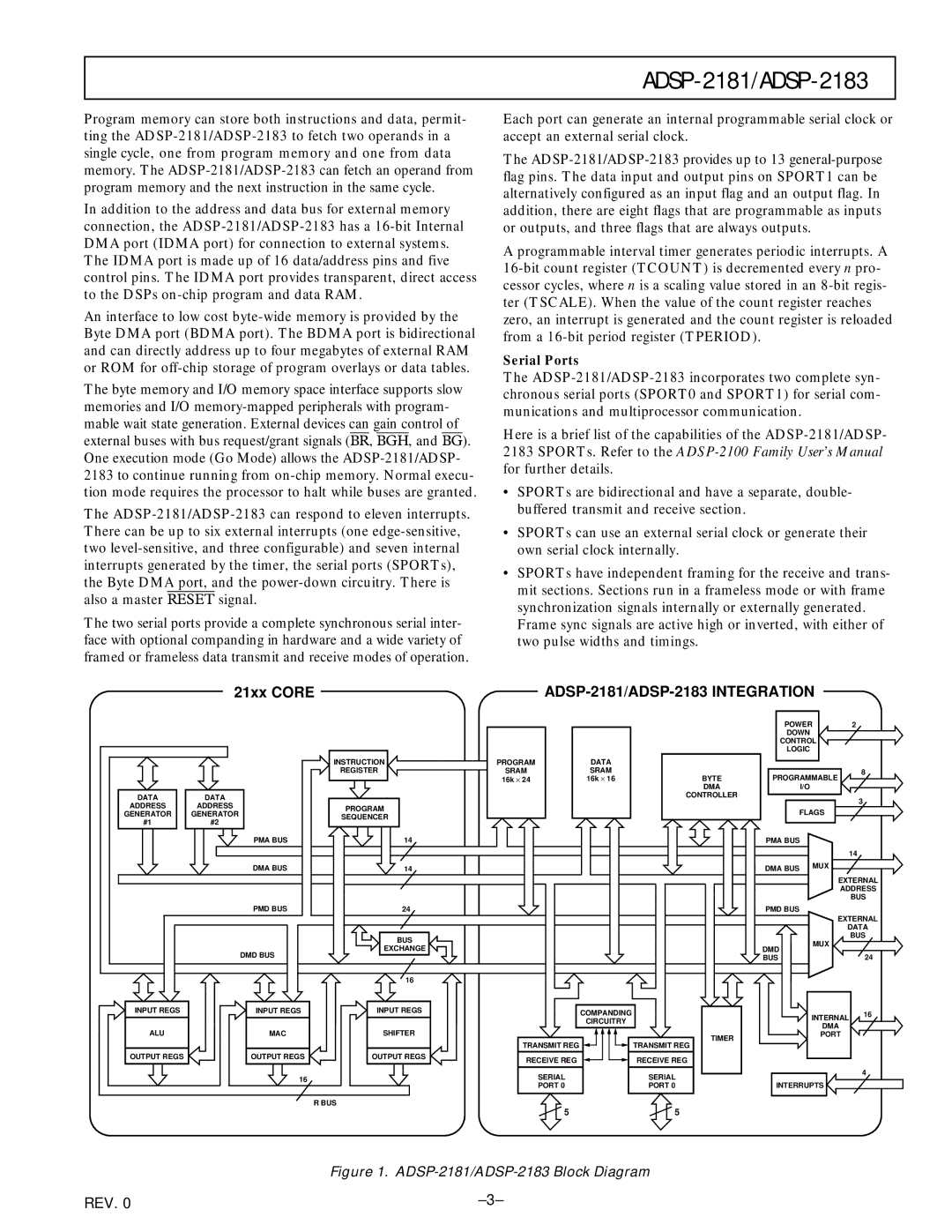
Figure 1. ADSP-2181/ADSP-2183 Block Diagram
REV. 0 |