ADSP-2181/ADSP-2183
When the IDLE (n) instruction is used, it effectively slows down the processor’s internal clock and thus its response time to in- coming interrupts. The
When the IDLE (n) instruction is used in systems that have an externally generated serial clock (SCLK), the serial clock rate may be faster than the processor’s reduced internal clock rate. Under these conditions, interrupts must not be generated at a faster rate than can be serviced, due to the additional time the processor takes to come out of the idle state (a maximum of n processor cycles).
SYSTEM INTERFACE
Figure 2 shows a typical basic system configuration with the ADSP-2181/ADSP-2183, two serial devices, a byte-wide EPROM, and optional external program and data overlay memories. Program-mable wait state generation allows the pro- cessor connects easily to slow peripheral devices. The ADSP- 2181/ADSP-2183 also provides four external interrupts and two serial ports or six external interrupts and one serial port.
The ADSP-2181/ADSP-2183 uses an input clock with a fre- quency equal to half the instruction rate; a 16.67 MHz input clock yields a 30 ns processor cycle (which is equivalent to
33 MHz). Normally, instructions are executed in a single pro- cessor cycle. All device timing is relative to the internal instruc- tion clock rate, which is indicated by the CLKOUT signal when enabled.
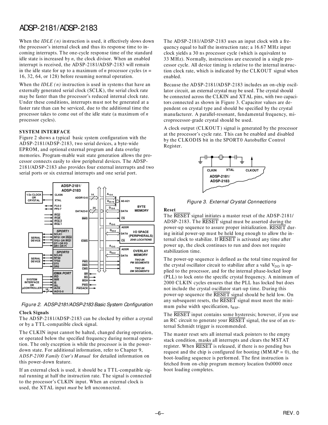
Because the ADSP-2181/ADSP-2183 includes an on-chip oscil- lator circuit, an external crystal may be used. The crystal should be connected across the CLKIN and XTAL pins, with two capaci- tors connected as shown in Figure 3. Capacitor values are de- pendent on crystal type and should be specified by the crystal manufacturer. A parallel-resonant, fundamental frequency, mi- croprocessor-grade crystal should be used.
A clock output (CLKOUT) signal is generated by the processor at the processor’s cycle rate. This can be enabled and disabled by the CLKODIS bit in the SPORT0 Autobuffer Control Register.
CLKIN XTAL CLKOUT
ADSP-2181/
ADSP-2183
|
|
|
|
|
|
|
|
| |||||||||||||
|
|
|
|
|
|
|
|
| |||||||||||||
1/2x CLOCK |
|
|
|
|
|
| CLKIN | 14 | |||||||||||||
|
|
|
|
| |||||||||||||||||
| OR |
|
|
|
|
|
| XTAL | |||||||||||||
CRYSTAL |
|
|
|
|
|
|
|
|
|
|
|
|
| ||||||||
|
|
|
|
|
|
|
|
|
|
|
| ||||||||||
|
|
|
|
|
|
|
| 24 | |||||||||||||
|
|
|
|
|
|
|
| ||||||||||||||
|
|
|
|
|
|
| |||||||||||||||
|
|
|
|
|
|
|
| ||||||||||||||
|
|
|
|
|
|
|
| ||||||||||||||
|
|
|
|
|
|
|
|
|
|
|
|
|
|
| |||||||
|
|
|
|
|
|
|
|
|
|
|
|
|
|
|
|
|
| ||||
|
|
|
|
|
|
|
| IRQ2 |
|
|
|
|
|
|
| ||||||
|
|
|
|
|
|
|
|
|
|
|
|
|
| ||||||||
|
|
|
|
|
|
|
| IRQE |
|
|
|
|
|
|
| ||||||
|
|
|
|
|
|
|
|
|
| BMS | |||||||||||
|
|
|
|
|
|
| |||||||||||||||
|
|
|
|
|
|
|
| IRQL0 |
|
|
|
|
|
|
|
| |||||
|
|
|
|
|
|
|
|
|
|
|
|
|
| ||||||||
|
|
|
|
|
|
|
| IRQL1 |
|
|
|
|
|
|
| ||||||
|
|
|
|
|
|
|
|
|
|
|
|
|
| ||||||||
|
|
|
|
|
|
|
|
|
|
|
|
|
|
|
|
|
|
|
|
|
|
|
|
|
|
|
|
|
| SPORT1 |
|
|
|
|
|
|
| ||||||
|
|
|
|
|
|
| SCLK1 |
|
|
|
|
|
|
| |||||||
| SERIAL |
|
|
|
|
| RFS1 OR | IRQ0 |
|
|
|
|
|
|
|
| |||||
|
|
|
|
|
|
|
|
|
|
| |||||||||||
| DEVICE |
|
|
|
|
| TFS1 OR | IRQ1 |
|
| IOMS |
|
|
| |||||||
|
|
|
|
|
|
| DT1 OR FO |
|
|
|
|
|
|
| |||||||
|
|
|
|
|
|
|
|
|
|
|
|
|
| ||||||||
|
|
|
|
|
|
| DR1 OR FI |
|
|
|
|
|
|
| |||||||
|
|
|
|
|
|
|
|
|
|
|
|
|
| ||||||||
|
|
|
|
|
|
|
|
|
|
|
|
|
|
|
|
|
| ||||
|
|
|
|
|
|
|
| SPORT0 |
|
|
|
|
|
|
| ||||||
|
|
|
|
|
|
| SCLK0 |
|
|
|
|
|
|
| |||||||
| SERIAL |
|
|
|
|
| RFS0 |
|
|
|
|
|
|
| |||||||
|
|
|
|
|
|
|
|
|
|
|
|
| |||||||||
| DEVICE |
|
|
|
|
| TFS0 |
|
| PMS |
|
| |||||||||
|
|
|
|
|
| ||||||||||||||||
|
|
|
|
|
|
| DT0 |
|
|
|
|
|
|
| |||||||
|
|
|
|
|
|
|
|
| DMS | ||||||||||||
|
|
|
|
|
|
| DR0 |
|
| ||||||||||||
|
|
|
|
|
|
|
|
|
|
|
|
|
| ||||||||
|
|
|
|
|
|
|
|
| CMS | ||||||||||||
|
|
|
|
|
|
|
|
|
|
|
|
|
|
|
|
| |||||
|
| IDMA PORT | BR |
SYSTEM |
| IRD | BG |
| IWR | BGH | |
INTERFACE |
| IS | |
| PWD | ||
OR |
| IAL | |
µCONTROLLER | 16 | IACK | PWDACK |
|
| ||
|
|
|
|
|
|
|
| |||
|
| ||||||
|
| ||||||
|
|
|
| BYTE | |||
| DATA | MEMORY | |||||
|
|
|
| ||||
|
|
|
|
|
|
|
|
|
|
|
|
| CS |
| |
|
|
|
|
| |||
|
|
|
|
|
|
|
|
|
|
|
|
| |||
|
| ADDR | I/O SPACE | ||||
| DATA | ||||||
|
|
|
| ||||
|
|
|
| (PERIPHERALS) | |||
|
|
|
|
|
|
| |
|
|
|
|
|
|
| 2048 LOCATIONS |
|
|
|
|
| CS | ||
|
|
| |||||
|
|
|
|
| |||
|
|
|
|
| |||
|
| ADDR | OVERLAY | ||||
|
|
|
| ||||
| DATA | MEMORY | |||||
|
|
|
| ||||
|
|
|
|
|
|
| TWO 8K |
|
|
|
|
|
|
| PM SEGMENTS |
|
|
|
|
|
|
| TWO 8K |
|
|
|
|
|
|
| |
|
|
|
|
|
|
| |
|
|
|
|
|
|
| DM SEGMENTS |
|
|
|
|
|
|
|
|
Figure 3. External Crystal Connections
Reset
The RESET signal initiates a master reset of the
The
Figure 2. ADSP-2181/ADSP-2183 Basic System Configuration
Clock Signals
The
The CLKIN input cannot be halted, changed during operation, or operated below the specified frequency during normal opera- tion. The only exception is while the processor is in the power- down state. For additional information, refer to Chapter 9,
If an external clock is used, it should be a
mum pulse width specification, tRSP.
The RESET input contains some hysteresis; however, if you use an RC circuit to generate your RESET signal, the use of an ex- ternal Schmidt trigger is recommended.
The master reset sets all internal stack pointers to the empty stack condition, masks all interrupts and clears the MSTAT register. When RESET is released, if there is no pending bus request and the chip is configured for booting (MMAP = 0), the
REV. 0 |