CHAPTER 2. TECHNICAL DESCRIPTION
2.2 Signal Processing
| MAIN PCB ASS'Y |
| ||
|
| SDRAM |
| |
|
|
| CF card | |
| Drive | HD, VD |
| |
| Pulse | CLK |
| |
| TG |
|
| |
|
| DSP |
| |
CCD |
| LCD | LCD | |
CDS, A/D | Driver | |||
Sensor |
| |||
|
|
| ||
EF LENS | Motor | Video |
| |
Driver | VIDEO OUT | |||
| Amp | |||
|
|
| ||
|
|
| AUDIO OUT | |
AF Support LED |
|
|
| |
|
| FLASH MEMORY |
| |
FINDER LED |
|
|
| |
|
|
| USB | |
|
| CPU |
| |
| RTC |
|
| |
|
|
| SW | |
Electric FLASH |
|
| DIAL | |
|
|
| KEY | |
MIC |
| AUDIO AMP |
| |
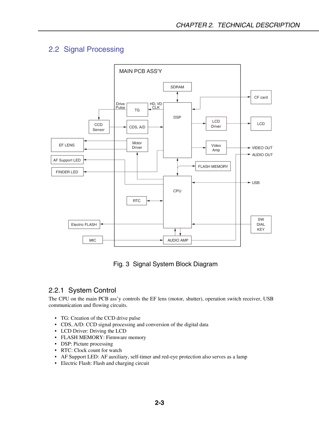
Fig. 3 Signal System Block Diagram
2.2.1 System Control
The CPU on the main PCB ass’y controls the EF lens (motor, shutter), operation switch receiver, USB communication and flowing circuits.
•TG: Creation of the CCD drive pulse
•CDS, A/D: CCD signal processing and conversion of the digital data
•LCD Driver: Driving the LCD
•FLASH MEMORY: Firmware memory
•DSP: Picture processing
•RTC: Clock count for watch
•AF Support LED: AF auxiliary,
•Electric Flash: Flash and charging circuit