CHAPTER 2. TECHNICAL DESCRIPTION
2.Outline of Circuits
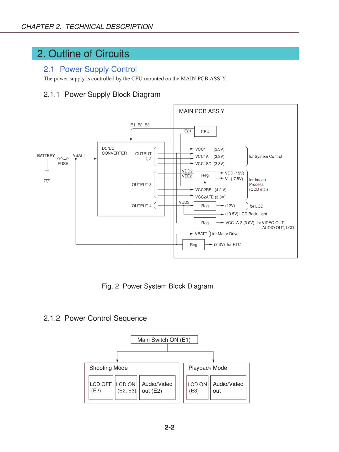
2.1Power Supply Control
The power supply is controlled by the CPU mounted on the MAIN PCB ASS’Y.
2.1.1 Power Supply Block Diagram
BATTERYVBATT
FUSE
E1, E2, E3
DC/DC
CONVERTER OUTPUT 1, 2
OUTPUT 3
OUTPUT 4
MAIN PCB ASS'Y
|
|
|
| E21 | CPU |
|
|
|
|
|
| |||
|
|
|
|
|
|
|
|
|
|
|
|
|
|
|
|
|
|
|
|
|
| VCC1 | (3.3V) |
| |||||
|
|
|
|
|
|
|
| |||||||
|
|
|
|
|
|
|
| |||||||
|
|
|
|
|
|
| VCC1A | (3.3V) | for System Control | |||||
|
|
|
|
|
|
| ||||||||
|
|
|
|
|
|
| VCC1SD (3.3V) |
| ||||||
|
|
| VDD2 |
|
| |||||||||
|
|
|
|
|
|
|
|
|
| VDD (15V) |
| |||
|
|
| VEE2 |
| Reg |
|
|
|
|
| ||||
|
|
|
|
|
|
|
| VL | for Image | |||||
|
|
|
|
|
|
|
|
|
|
|
|
| ||
|
|
|
|
|
|
|
|
|
|
| ||||
|
|
|
|
|
|
|
|
|
|
|
|
|
| Process |
|
|
|
|
|
|
|
|
|
|
|
|
|
| |
|
|
|
|
|
|
| VCC2RE | (4.2 V) | (CCD etc.) | |||||
|
|
|
|
|
|
| ||||||||
|
|
|
|
|
|
| VCC2AFE (3.3V) |
| ||||||
|
| VDD3 |
|
| ||||||||||
|
|
|
|
|
|
|
|
| (12V) |
| ||||
| Reg |
|
|
|
| for LCD | ||||||||
|
|
|
|
|
|
|
|
|
|
| ||||
|
|
|
|
|
|
|
|
|
|
| ||||
|
|
|
|
|
|
|
|
|
|
|
|
| (13.5V) LCD Back Light | |
|
|
|
|
|
|
|
|
|
|
|
|
| ||
|
|
|
|
|
|
|
|
|
|
|
|
| ||
|
|
|
|
|
|
| Reg |
|
|
|
| |||
|
|
|
|
|
|
|
|
|
| |||||
|
|
|
|
|
|
|
|
|
|
|
|
|
| AUDIO OUT, LCD |
|
|
|
|
|
|
| VBATT | for Motor Drive | ||||||
|
|
|
|
|
|
|
| |||||||
|
|
|
|
|
|
|
| |||||||
Reg
![]() (3.3V) for RTC
(3.3V) for RTC
Fig. 2 Power System Block Diagram
2.1.2 Power Control Sequence
Main Switch ON (E1)
Shooting Mode
LCD OFF |
| LCD ON |
(E2) |
| (E2, E3) |
|
|
|
Audio/Video out (E2)
Playback Mode
LCD ON |
| Audio/Video |
(E3) |
| out |
|
|
|