CHAPTER 2. TECHNICAL DESCRIPTION
3.Troubleshooting
3.1When an Error Code is Displayed
[Remedy]
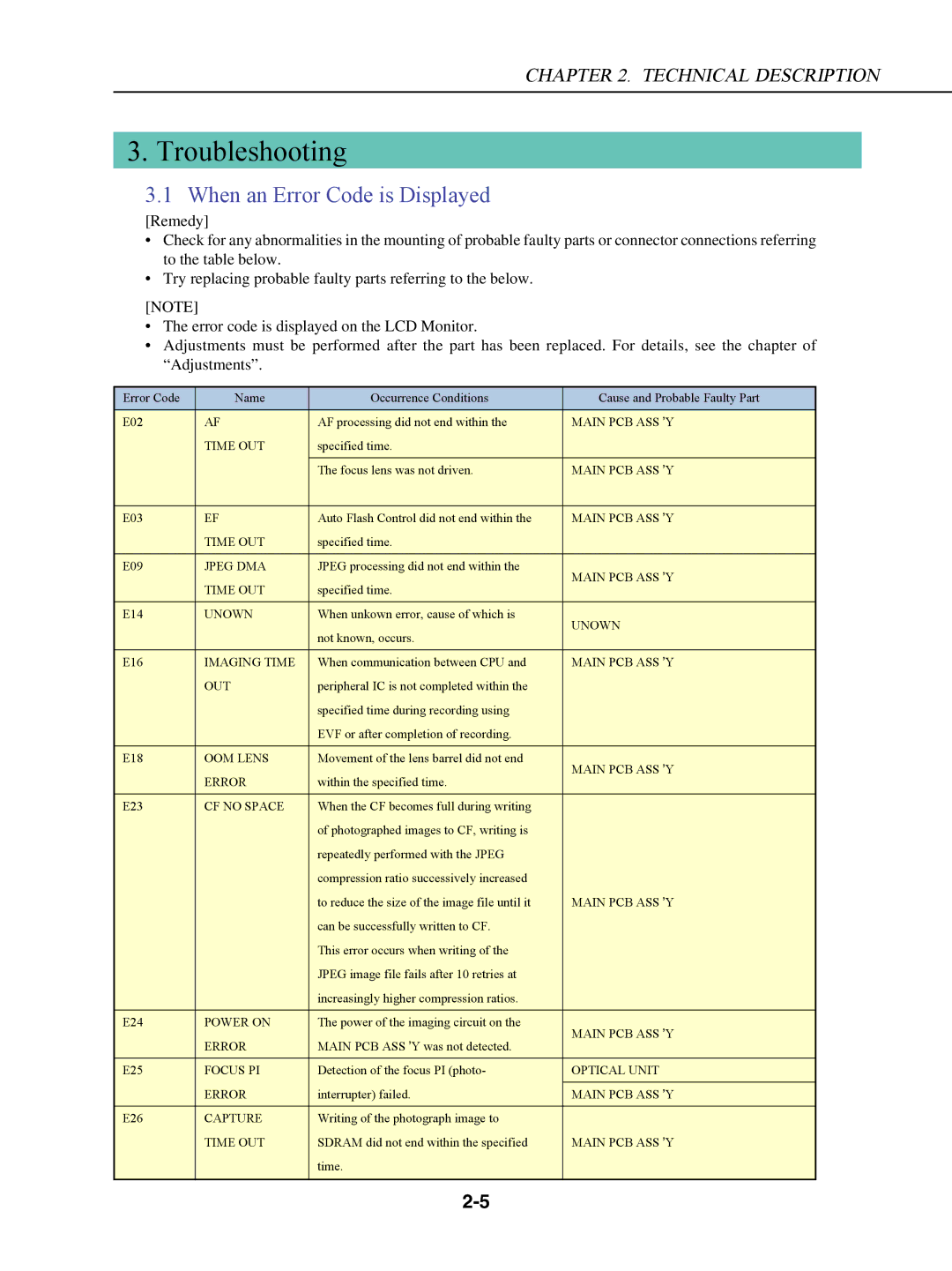
•Check for any abnormalities in the mounting of probable faulty parts or connector connections referring to the table below.
•Try replacing probable faulty parts referring to the below.
[NOTE]
•The error code is displayed on the LCD Monitor.
•Adjustments must be performed after the part has been replaced. For details, see the chapter of “Adjustments”.
Error Code | Name | Occurrence Conditions | Cause and Probable Faulty Part |
E02 | AF | AF processing did not end within the | MAIN PCB ASS’Y |
| TIME OUT | specified time. |
|
|
| The focus lens was not driven. | MAIN PCB ASS’Y |
|
|
|
|
E03 | EF | Auto Flash Control did not end within the | MAIN PCB ASS’Y |
| TIME OUT | specified time. |
|
E09 | JPEG DMA | JPEG processing did not end within the | MAIN PCB ASS’Y |
| TIME OUT | specified time. | |
|
| ||
E14 | UNKOWN | When unkown error, cause of which is | UNKOWN |
|
| not known, occurs. | |
|
|
| |
E16 | IMAGING TIME | When communication between CPU and | MAIN PCB ASS’Y |
| OUT | peripheral IC is not completed within the |
|
|
| specified time during recording using |
|
|
| EVF or after completion of recording. |
|
E18 | ZOOM LENS | Movement of the lens barrel did not end | MAIN PCB ASS’Y |
| ERROR | within the specified time. | |
|
| ||
E23 | CF NO SPACE | When the CF becomes full during writing |
|
|
| of photographed images to CF, writing is |
|
|
| repeatedly performed with the JPEG |
|
|
| compression ratio successively increased |
|
|
| to reduce the size of the image file until it | MAIN PCB ASS’Y |
|
| can be successfully written to CF. |
|
|
| This error occurs when writing of the |
|
|
| JPEG image file fails after 10 retries at |
|
|
| increasingly higher compression ratios. |
|
E24 | POWER ON | The power of the imaging circuit on the | MAIN PCB ASS’Y |
| ERROR | MAIN PCB ASS’Y was not detected. | |
|
| ||
E25 | FOCUS PI | Detection of the focus PI (photo- | OPTICAL UNIT |
| ERROR | interrupter) failed. | MAIN PCB ASS’Y |
E26 | CAPTURE | Writing of the photograph image to |
|
| TIME OUT | SDRAM did not end within the specified | MAIN PCB ASS’Y |
|
| time. |
|
|
|
|
|
