PRELIMINARY CY8CNP102B, CY8CNP102E
DC Electrical Characteristics
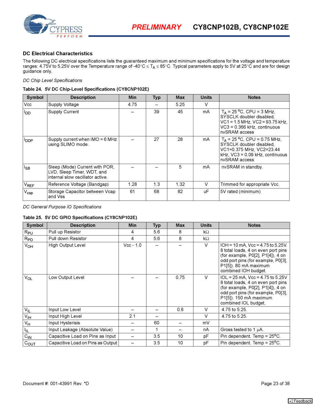
The following DC electrical specifications lists the guaranteed maximum and minimum specifications for the voltage and temperature ranges: 4.75V to 5.25V over the Temperature range of
DC Chip Level Specifications
Table 24. 5V DC
Symbol | Description | Min | Typ | Max | Units | Notes |
Vcc | Supply Voltage | 4.75 | – | 5.25 | V |
|
|
|
|
|
|
|
|
I | Supply Current | – | 39 | 45 | mA | T = 25 oC, CPU = 3 MHz, |
DD |
|
|
|
|
| A |
|
|
|
|
|
| SYSCLK doubler disabled, |
|
|
|
|
|
| VC1 = 1.5 MHz, VC2 = 93.75 kHz, |
|
|
|
|
|
| VC3 = 0.366 kHz, continuous |
|
|
|
|
|
| nvSRAM access |
I | Supply current when IMO = 6 MHz | – | 27 | 28 | mA | T = 25 oC, CPU = 0.75 MHz, |
DDP | using SLIMO mode. |
|
|
|
| A |
|
|
|
|
| SYSCLK doubler disabled, | |
|
|
|
|
|
| VC1=0.375 MHz, VC2=23.44 |
|
|
|
|
|
| kHz, VC3 = 0.09 kHz, continuous |
|
|
|
|
|
| nvSRAM access |
ISB | Sleep (Mode) Current with POR, | – | – | 5 | mA | nvSRAM in standby. |
| LVD, Sleep Timer, WDT, and |
|
|
|
|
|
| internal slow oscillator active. |
|
|
|
|
|
VREF | Reference Voltage (Bandgap) | 1.28 | 1.3 | 1.32 | V | Trimmed for appropriate Vcc. |
Vcap | Storage Capacitor between Vcap | 61 | 68 | 82 | uF | 5V rated (minimum) |
| and Vss |
|
|
|
|
|
DC General Purpose IO Specifications |
|
|
|
|
| |
Table 25. 5V DC GPIO Specifications (CY8CNP102E) |
|
|
|
| ||
|
|
|
|
|
|
|
Symbol | Description | Min | Typ | Max | Units | Notes |
RPU | Pull up Resistor | 4 | 5.6 | 8 | kΩ |
|
RPD | Pull down Resistor | 4 | 5.6 | 8 | kΩ |
|
VOH | High Output Level | Vcc - 1.0 | – | – | V | IOH = 10 mA, Vcc = 4.75 to 5.25V. |
|
|
|
|
|
| 8 total loads, 4 on even port pins |
|
|
|
|
|
| (for example, P0[2], P1[4]), 4 on |
|
|
|
|
|
| odd port pins (for example, P0[3], |
|
|
|
|
|
| P1[5]). 80 mA maximum |
|
|
|
|
|
| combined IOH budget. |
VOL | Low Output Level | – | – | 0.75 | V | IOL = 25 mA, Vcc = 4.75 to 5.25V |
|
|
|
|
|
| 8 total loads, 4 on even port pins |
|
|
|
|
|
| (for example, P0[2], P1[4]), 4 on |
|
|
|
|
|
| odd port pins (for example, P0[3], |
|
|
|
|
|
| P1[5]). 150 mA maximum |
|
|
|
|
|
| combined IOL budget. |
VIL | Input Low Level | – | – | 0.8 | V | 4.75 to 5.25. |
VIH | Input High Level | 2.1 | – |
| V | 4.75 to 5.25. |
VH | Input Hysterisis | – | 60 | – | mV |
|
IIL | Input Leakage (Absolute Value) | – | 1 | – | nA | Gross tested to 1 μA. |
CIN | Capacitive Load on Pins as Input | – | 3.5 | 10 | pF | Pin dependent. Temp = 25oC. |
COUT | Capacitive Load on Pins as Output | – | 3.5 | 10 | pF | Pin dependent. Temp = 25oC. |
Document #: | Page 23 of 38 |
[+] Feedback