PRELIMINARY CY8CNP102B, CY8CNP102E
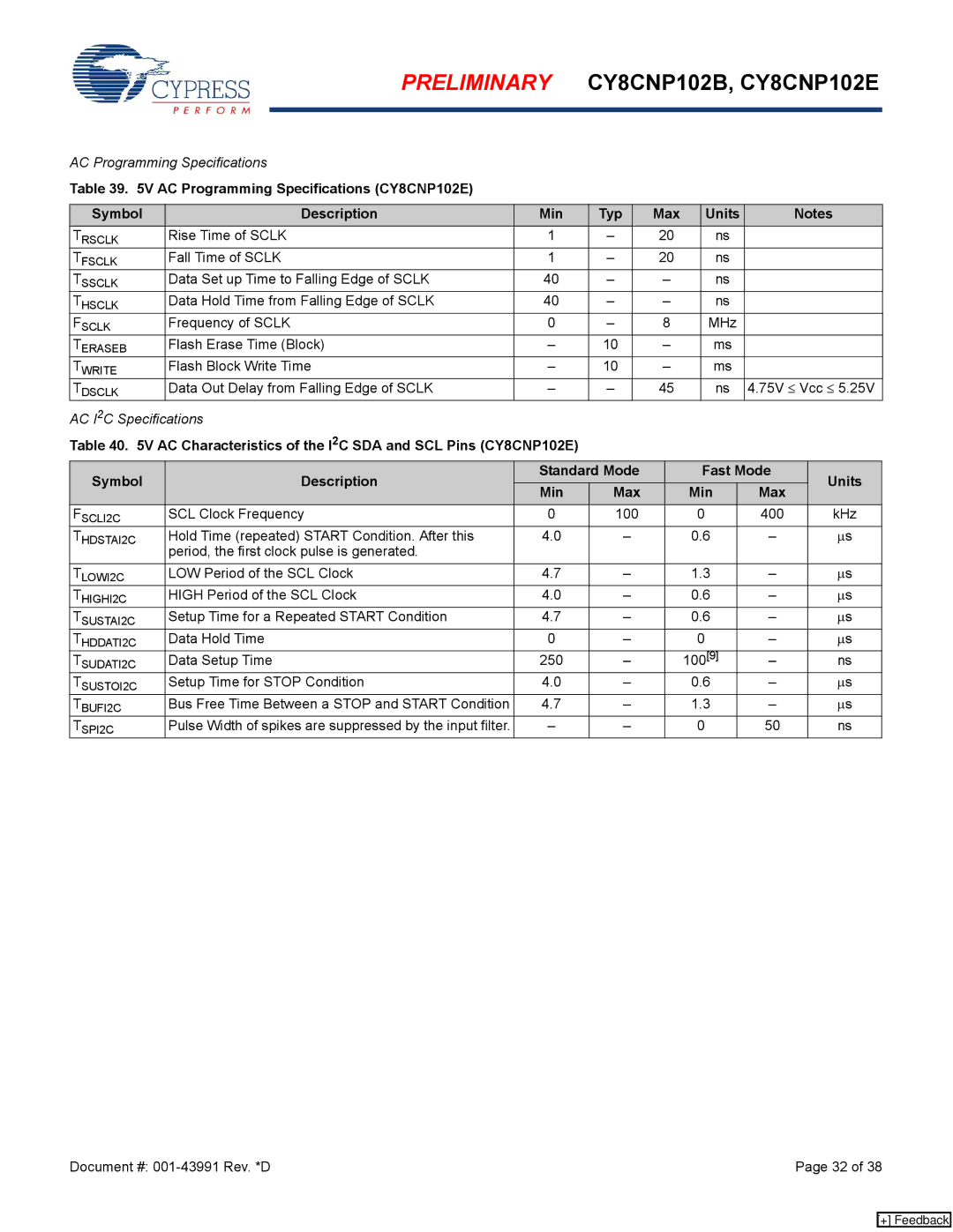
AC Programming Specifications
Table 39. 5V AC Programming Specifications (CY8CNP102E)
Symbol | Description | Min | Typ | Max | Units | Notes |
TRSCLK | Rise Time of SCLK | 1 | – | 20 | ns |
|
TFSCLK | Fall Time of SCLK | 1 | – | 20 | ns |
|
TSSCLK | Data Set up Time to Falling Edge of SCLK | 40 | – | – | ns |
|
THSCLK | Data Hold Time from Falling Edge of SCLK | 40 | – | – | ns |
|
FSCLK | Frequency of SCLK | 0 | – | 8 | MHz |
|
TERASEB | Flash Erase Time (Block) | – | 10 | – | ms |
|
TWRITE | Flash Block Write Time | – | 10 | – | ms |
|
TDSCLK | Data Out Delay from Falling Edge of SCLK | – | – | 45 | ns | 4.75V ≤ Vcc ≤ 5.25V |
AC I2C Specifications |
|
|
|
|
| |
Table 40. 5V AC Characteristics of the I2C SDA and SCL Pins (CY8CNP102E) |
|
|
|
| ||
Symbol | Description | Standard Mode | Fast Mode | Units | |||
Min | Max | Min | Max | ||||
|
|
| |||||
FSCLI2C | SCL Clock Frequency | 0 | 100 | 0 | 400 | kHz | |
THDSTAI2C | Hold Time (repeated) START Condition. After this | 4.0 | – | 0.6 | – | μs | |
| period, the first clock pulse is generated. |
|
|
|
|
| |
TLOWI2C | LOW Period of the SCL Clock | 4.7 | – | 1.3 | – | μs | |
THIGHI2C | HIGH Period of the SCL Clock | 4.0 | – | 0.6 | – | μs | |
TSUSTAI2C | Setup Time for a Repeated START Condition | 4.7 | – | 0.6 | – | μs | |
THDDATI2C | Data Hold Time | 0 | – | 0 | – | μs | |
T | Data Setup Time | 250 | – | 100[9] | – | ns | |
SUDATI2C |
|
|
|
|
|
| |
TSUSTOI2C | Setup Time for STOP Condition | 4.0 | – | 0.6 | – | μs | |
TBUFI2C | Bus Free Time Between a STOP and START Condition | 4.7 | – | 1.3 | – | μs | |
TSPI2C | Pulse Width of spikes are suppressed by the input filter. | – | – | 0 | 50 | ns | |
Document #: | Page 32 of 38 |
[+] Feedback