PRELIMINARY CY8CNP102B, CY8CNP102E
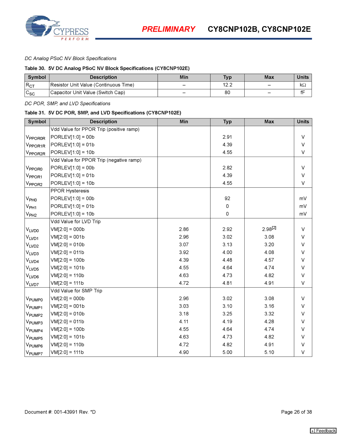
DC Analog PSoC NV Block Specifications
Table 30. 5V DC Analog PSoC NV Block Specifications (CY8CNP102E)
Symbol | Description | Min | Typ | Max | Units |
RCT | Resistor Unit Value (Continuous Time) | – | 12.2 | – | kΩ |
CSC | Capacitor Unit Value (Switch Cap) | – | 80 | – | fF |
DC POR, SMP, and LVD Specifications |
|
|
|
| |
Table 31. 5V DC POR, SMP, and LVD Specifications (CY8CNP102E) |
|
|
| ||
|
|
|
|
|
|
Symbol | Description | Min | Typ | Max | Units |
| Vdd Value for PPOR Trip (positive ramp) |
|
|
|
|
VPPOR0R | PORLEV[1:0] = 00b |
| 2.91 |
| V |
VPPOR1R | PORLEV[1:0] = 01b |
| 4.39 |
| V |
VPPOR2R | PORLEV[1:0] = 10b |
| 4.55 |
| V |
| Vdd Value for PPOR Trip (negative ramp) |
|
|
|
|
VPPOR0 | PORLEV[1:0] = 00b |
| 2.82 |
| V |
VPPOR1 | PORLEV[1:0] = 01b |
| 4.39 |
| V |
VPPOR2 | PORLEV[1:0] = 10b |
| 4.55 |
| V |
| PPOR Hysteresis |
|
|
|
|
VPH0 | PORLEV[1:0] = 00b |
| 92 |
| mV |
VPH1 | PORLEV[1:0] = 01b |
| 0 |
| mV |
VPH2 | PORLEV[1:0] = 10b |
| 0 |
| mV |
| Vdd Value for LVD Trip |
|
|
|
|
VLVD0 | VM[2:0] = 000b | 2.86 | 2.92 | 2.98[2] | V |
VLVD1 | VM[2:0] = 001b | 2.96 | 3.02 | 3.08 | V |
VLVD2 | VM[2:0] = 010b | 3.07 | 3.13 | 3.20 | V |
VLVD3 | VM[2:0] = 011b | 3.92 | 4.00 | 4.08 | V |
VLVD4 | VM[2:0] = 100b | 4.39 | 4.48 | 4.57 | V |
VLVD5 | VM[2:0] = 101b | 4.55 | 4.64 | 4.74 | V |
VLVD6 | VM[2:0] = 110b | 4.63 | 4.73 | 4.82 | V |
VLVD7 | VM[2:0] = 111b | 4.72 | 4.81 | 4.91 | V |
| Vdd Value for SMP Trip |
|
|
|
|
VPUMP0 | VM[2:0] = 000b | 2.96 | 3.02 | 3.08 | V |
VPUMP1 | VM[2:0] = 001b | 3.03 | 3.10 | 3.16 | V |
VPUMP2 | VM[2:0] = 010b | 3.18 | 3.25 | 3.32 | V |
VPUMP3 | VM[2:0] = 011b | 4.11 | 4.19 | 4.28 | V |
VPUMP4 | VM[2:0] = 100b | 4.55 | 4.64 | 4.74 | V |
VPUMP5 | VM[2:0] = 101b | 4.63 | 4.73 | 4.82 | V |
VPUMP6 | VM[2:0] = 110b | 4.72 | 4.82 | 4.91 | V |
VPUMP7 | VM[2:0] = 111b | 4.90 | 5.00 | 5.10 | V |
Document #: | Page 26 of 38 |
[+] Feedback