PRELIMINARY CY8CNP102B, CY8CNP102E
DC Analog Output Buffer Specifications
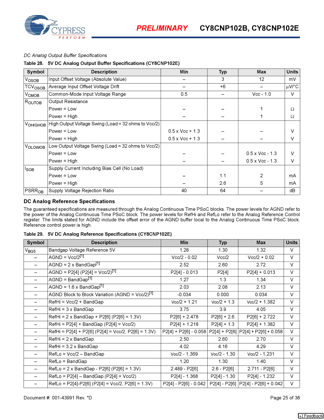
Table 28. 5V DC Analog Output Buffer Specifications (CY8CNP102E)
Symbol | Description | Min | Typ | Max | Units |
VOSOB | Input Offset Voltage (Absolute Value) | – | 3 | 12 | mV |
TCVOSOB | Average Input Offset Voltage Drift | – | +6 | – | μV/°C |
VCMOB | 0.5 | – | Vcc - 1.0 | V | |
ROUTOB | Output Resistance |
|
|
|
|
| Power = Low | – | – | 1 | Ω |
| Power = High | – | – | 1 | Ω |
|
|
|
|
|
|
VOHIGHOB | High Output Voltage Swing (Load = 32 ohms to Vcc/2) |
|
|
|
|
| Power = Low | 0.5 x Vcc + 1.3 | – | – | V |
| Power = High | 0.5 x Vcc + 1.3 | – | – | V |
|
|
|
|
|
|
VOLOWOB | Low Output Voltage Swing (Load = 32 ohms to Vcc/2) |
|
|
|
|
| Power = Low | – | – | 0.5 x Vcc - 1.3 | V |
| Power = High | – | – | 0.5 x Vcc - 1.3 | V |
|
|
|
|
|
|
ISOB | Supply Current Including Bias Cell (No Load) |
|
|
|
|
| Power = Low | – | 1.1 | 2 | mA |
| Power = High | – | 2.6 | 5 | mA |
|
|
|
|
|
|
PSRROB | Supply Voltage Rejection Ratio | 40 | 64 | – | dB |
DC Analog Reference Specifications
The guaranteed specifications are measured through the Analog Continuous Time PSoC blocks. The power levels for AGND refer to the power of the Analog Continuous Time PSoC block. The power levels for RefHi and RefLo refer to the Analog Reference Control register. The limits stated for AGND include the offset error of the AGND buffer local to the Analog Continuous Time PSoC block. Reference control power is high.
Table 29. 5V DC Analog Reference Specifications (CY8CNP102E)
Symbol | Description | Min | Typ | Max | Units |
VBG5 | Bandgap Voltage Reference 5V | 1.28 | 1.30 | 1.32 | V |
– | AGND = Vcc/2[1] | Vcc/2 - 0.02 | Vcc/2 | Vcc/2 + 0.02 | V |
– | AGND = 2 x BandGap[1] | 2.52 | 2.60 | 2.72 | V |
– | AGND = P2[4] (P2[4] = Vcc/2)[1] | P2[4] - 0.013 | P2[4] | P2[4] + 0.013 | V |
– | AGND = BandGap[1] | 1.27 | 1.3 | 1.34 | V |
– | AGND = 1.6 x BandGap[1] | 2.03 | 2.08 | 2.13 | V |
– | AGND Block to Block Variation (AGND = Vcc/2)[1] | 0.000 | 0.034 | V | |
– | RefHi = Vcc/2 + BandGap | Vcc/2 + 1.21 | Vcc/2 + 1.3 | Vcc/2 + 1.382 | V |
|
|
|
|
|
|
– | RefHi = 3 x BandGap | 3.75 | 3.9 | 4.05 | V |
|
|
|
|
|
|
– | RefHi = 2 x BandGap + P2[6] (P2[6] = 1.3V) | P2[6] + 2.478 | P2[6] + 2.6 | P2[6] + 2.722 | V |
|
|
|
|
|
|
– | RefHi = P2[4] + BandGap (P2[4] = Vcc/2) | P2[4] + 1.218 | P2[4] + 1.3 | P2[4] + 1.382 | V |
|
|
|
|
|
|
– | RefHi = P2[4] + P2[6] (P2[4] = Vcc/2, P2[6] = 1.3V) | P2[4] + P2[6] - 0.058 | P2[4] + P2[6] | P2[4] + P2[6] + 0.058 | V |
|
|
|
|
|
|
– | RefHi = 2 x BandGap | 2.50 | 2.60 | 2.70 | V |
|
|
|
|
|
|
– | RefHi = 3.2 x BandGap | 4.02 | 4.16 | 4.29 | V |
|
|
|
|
|
|
– | RefLo = Vcc/2 – BandGap | Vcc/2 - 1.369 | Vcc/2 - 1.30 | Vcc/2 - 1.231 | V |
|
|
|
|
|
|
– | RefLo = BandGap | 1.20 | 1.30 | 1.40 | V |
|
|
|
|
|
|
– | RefLo = 2 x BandGap - P2[6] (P2[6] = 1.3V) | 2.489 - P2[6] | 2.6 - P2[6] | 2.711 - P2[6] | V |
|
|
|
|
|
|
– | RefLo = P2[4] – BandGap (P2[4] = Vcc/2) | P2[4] - 1.368 | P2[4] - 1.30 | P2[4] - 1.232 | V |
|
|
|
|
|
|
– | RefLo = | P2[4] - P2[6] - 0.042 | P2[4] - P2[6] | P2[4] - P2[6] + 0.042 | V |
|
|
|
|
|
|
Document #: |
|
| Page 25 of 38 | ||
[+] Feedback