PRELIMINARY CY8CNP102B, CY8CNP102E
Table 1. Pin Definitions -
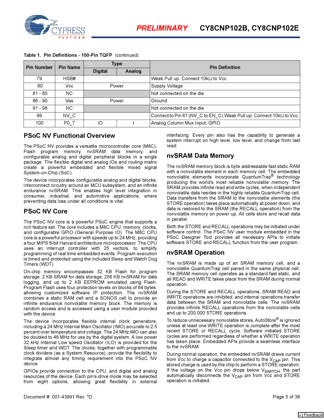
Pin Number | Pin Name |
| Type | Pin Definition | |
Digital |
| Analog | |||
|
|
|
| ||
79 | HSB# |
|
|
| Weak Pull up. Connect 10kΩ to Vcc. |
|
|
|
|
| |
80 | Vcc |
| Power | Supply Voltage | |
|
|
|
|
|
|
81 - 85 | NC |
|
|
| Not connected on the die |
86 - 90 | Vss |
| Power | Ground | |
|
|
|
|
|
|
91 - 98 | NC |
|
|
| Not connected on the die |
99 | NV_C |
|
|
| Connect to Pin 61 (NV_C to EN_C).Weak Pull up. Connect 10kΩ to Vcc. |
|
|
|
|
|
|
100 | P0_7 | IO |
| I | Analog Column Mux Input, GPIO |
|
|
|
|
|
|
PSoC NV Functional Overview
The PSoC NV provides a versatile microcontroller core (M8C), Flash program memory, nvSRAM data memory, and configurable analog and digital peripheral blocks in a single package. The flexible digital and analog IOs and routing matrix create a powerful embedded and flexible mixed signal
The device incorporates configurable analog and digital blocks, interconnect circuitry around an MCU subsystem, and an infinite endurance nvSRAM. This enables high level integration in consumer, industrial, and automotive applications, where preventing data loss under all conditions is vital.
PSoC NV Core
The PSoC NV core is a powerful PSoC engine that supports a rich feature set. The core includes a M8C CPU, memory, clocks, and configurable GPIO (General Purpose IO). The M8C CPU core is a powerful processor with speeds up to 24 MHz, providing
afour MIPS
The device incorporates flexible internal clock generators, including a 24 MHz Internal Main Oscillator (IMO) accurate to 2.5 percent over temperature and voltage. The 24 MHz IMO can also be doubled to 48 MHz for use by the digital system. A low power 32 kHz Internal Low speed Oscillator (ILO) is provided for the Sleep timer and WDT. The clocks, together with programmable clock dividers (as a System Resource), provide the flexibility to integrate almost any timing requirement into the PSoC NV device.
GPIOs provide connection to the CPU, and digital and analog resources of the device. Each pin’s drive mode may be selected from eight options, allowing great flexibility in external
interfacing. Every pin also has the capability to generate a system interrupt on high level, low level, and change from last read.
nvSRAM Data Memory
The nvSRAM memory block is byte addressable fast static RAM with a nonvolatile element in each memory cell. The embedded nonvolatile elements incorporate QuantumTrap® technology producing the world’s most reliable nonvolatile memory. The SRAM provides infinite read and write cycles, when independent nonvolatile data resides in the highly reliable QuantumTrap cell. Data transfers from the SRAM to the nonvolatile elements (the STORE operation) takes place automatically at power down, and data is restored to the SRAM (the RECALL operation) from the nonvolatile memory on power up. All cells store and recall data in parallel.
Both the STORE and RECALL operations may be initiated under software control. The PSoC NV user module embedded in the PSoC Designer Tool provides all necessary APIs to initiate software STORE and RECALL function from the user program.
nvSRAM Operation
The nvSRAM is made up of an SRAM memory cell, and a nonvolatile QuantumTrap cell paired in the same physical cell. The SRAM memory cell operates as a standard fast static, and all READ and WRITE takes place from the SRAM during normal operation.
During the STORE and RECALL operations, SRAM READ and WRITE operations are inhibited, and internal operations transfer data between the SRAM and nonvolatile cells. The nvSRAM provides infinite RECALL operations from the nonvolatile cells and up to 200,000 STORE operations.
To reduce unnecessary nonvolatile stores, AutoStore® is ignored unless at least one WRITE operation is complete after the most recent STORE or RECALL cycle. Software initiated STORE cycles are performed regardless of whether a WRITE operation has taken place. Embedded APIs provide a seamless interface to the nvSRAM.
During normal operation, the embedded nvSRAM draws current from Vcc to charge a capacitor connected to the VCAP pin. This stored charge is used by the chip to perform a STORE operation. If the voltage on the Vcc pin drops below VSWITCH, the part automatically disconnects the VCAP pin from Vcc and STORE operation is initiated.
Document #: | Page 5 of 38 |
[+] Feedback