Networking Silicon — 82555
11.0Electrical Specifications and Timing Parameters
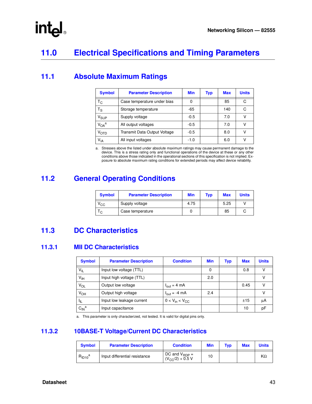
11.1Absolute Maximum Ratings
Symbol | Parameter Description | Min | Typ | Max | Units |
|
|
|
|
|
|
|
|
|
|
|
|
TC | Case temperature under bias | 0 |
| 85 | C |
TS | Storage temperature |
| 140 | C | |
VSUP | Supply voltage |
| 7.0 | V | |
a | All output voltages |
| 7.0 | V | |
VOA |
| ||||
VOTD | Transmit Data Output Voltage |
| 8.0 | V | |
VIA | All input voltages |
| 6.0 | V |
a. Stresses above the listed under absolute maximum ratings may cause permanent damage to the device. This is a stress rating only and functional operations of the device at these or any other conditions above those indicated in the operational sections of this specification is not implied. Ex- posure to absolute maximum rating conditions for extended periods may affect device reliability.
11.2 | General Operating Conditions |
|
|
|
| ||
|
|
|
|
|
|
|
|
|
| Symbol | Parameter Description | Min | Typ | Max | Units |
|
|
|
|
|
|
|
|
|
|
|
|
|
|
|
|
|
| VCC | Supply voltage | 4.75 |
| 5.25 | V |
|
| TC | Case temperature | 0 |
| 85 | C |
11.3 | DC Characteristics |
|
|
|
| ||
11.3.1MII DC Characteristics
Symbol | Parameter Description | Condition | Min | Typ | Max | Units |
|
|
|
|
|
|
|
|
|
|
|
|
|
|
VIL | Input low voltage (TTL) |
| 0 |
| 0.8 | V |
VIH | Input high voltage (TTL) |
| 2.0 |
|
| V |
VOL | Output low voltage | Iout = 4 mA |
|
| 0.45 | V |
VOH | Output high voltage | Iout = | 2.4 |
|
| V |
IIL | Input low leakage current | 0 < Vin < VCC |
|
| ±15 | μA |
CINa | Input capacitance |
|
|
| 10 | pF |
a.This parameter is only characterized, not tested. It is valid for digital pins only.
11.3.210BASE-T Voltage/Current DC Characteristics
Symbol | Parameter Description | Condition | Min | Typ | Max | Units |
|
|
|
|
|
|
|
|
|
|
|
|
|
|
a | Input differential resistance | DC and VRDP = | 10 |
|
| KΩ |
RID10 | (VCC/2) + 0.5 V |
|
| |||
|
|
|
|
|
|
Datasheet | 43 |