82555 — Networking Silicon
Symbol | Parameter Description | Condition | Min | Typ | Max | Units |
|
|
|
|
|
|
|
|
|
|
|
|
|
|
VIDA10 | Input differential accept voltage | 5 MHz ≤ f ≤ 10 MHz | ±585 |
| ±3100 | mVP |
VIDR10 | Input differential reject voltage | 5 MHz ≤ f ≤ 10 MHz |
|
| ±300 | mVP |
VICM10 | Input common mode voltage |
|
| VCC/2 |
| V |
VOD10 | Output differential voltage | RL = 100 Ωb | ±2.2 |
| ±2.8 | V |
RBIAS10 = 768 Ω |
| |||||
|
|
|
|
|
| |
|
|
|
|
|
|
|
c | Line driver supply | RBIAS10 = 768 Ω |
| 110 |
| mA |
ICCT10 |
|
| ||||
d | Current on all VCC pins |
|
| 120 |
| mA |
ICC10 |
|
|
| |||
ICCT10TOT | Total supply current |
|
| 230 |
| mA |
e | Leakage on analog pins |
|
|
| 20 | mA |
LILA10 |
|
|
|
a.This value is measured across the receive differential pins, RDP and RDN.
b.RL is the resistive load across the receive differential pins, RDP and RDN.
c.Transmitter current is measured with a 1:1 transformer on the center tap.
d.Current is measured on all VCC pins at VCC = 5.25 V.
e.The analog pins are: TDP, TDN, RDP, RDN, RBIAS10, and RBIAS100.
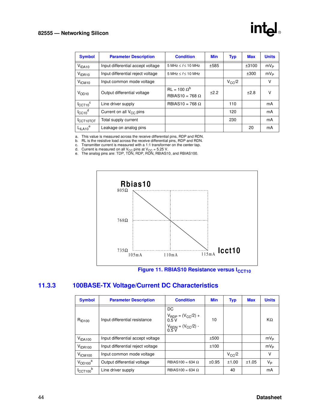
Rbias10
8 0 5 Ω
7 6 8 Ω
7 3 5 Ω |
| 1 1 5 m A Icct10 |
1 0 5 m A | 1 1 0 m A |
Figure 11. RBIAS10 Resistance versus ICCT10
11.3.3100BASE-TX Voltage/Current DC Characteristics
Symbol | Parameter Description | Condition | Min | Typ | Max | Units |
|
|
|
|
|
|
|
|
|
|
|
|
|
|
|
| DC |
|
|
|
|
RID100 | Input differential resistance | VRDP = (VCC/2) + | 10 |
|
| KΩ |
0.5 V |
|
| ||||
|
| VRDN = (VCC/2) - |
|
|
|
|
|
| 0.5 V |
|
|
|
|
|
|
|
|
|
|
|
VIDA100 | Input differential accept voltage |
| ±500 |
|
| mVP |
VIDR100 | Input differential reject voltage |
| ±100 |
|
| mVP |
VICM100 | Input common mode voltage |
|
| VCC/2 |
| V |
a | Output differential voltage | RBIAS100 = 634 Ω | ±0.95 | ±1.00 | ±1.05 | VP |
VOD100 | ||||||
b | Line driver supply | RBIAS100 = 634 Ω |
| 40 |
| mA |
ICCT100 |
|
|
44 | Datasheet |
