A
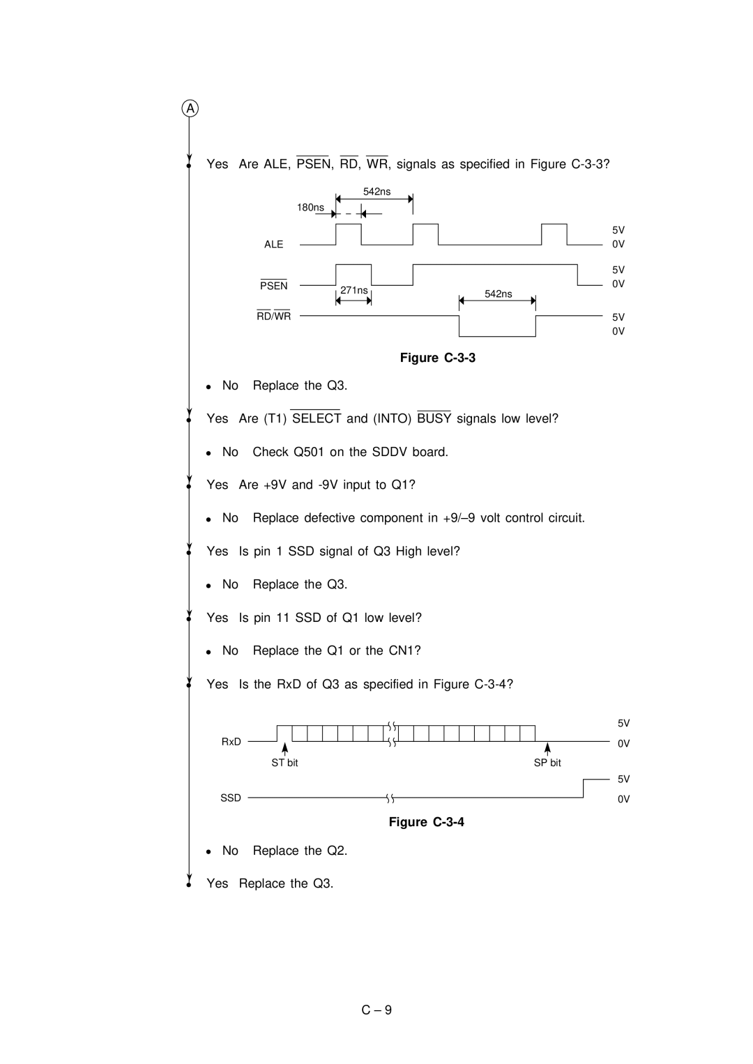
Yes Are ALE, PSEN, RD, WR, signals as specified in Figure
542ns
180ns
ALE
|
|
|
|
|
|
|
|
|
|
|
|
|
|
|
|
|
|
|
|
|
|
|
|
|
|
|
|
|
|
|
|
|
|
|
|
|
|
|
|
|
|
|
| PSEN |
|
|
|
| 271ns |
|
|
|
|
|
|
|
|
|
|
|
|
| 542ns |
|
|
|
|
| |||||||||||||
|
|
|
|
|
|
|
|
|
|
|
|
|
|
|
|
|
|
|
|
|
|
| ||||||||||||||||||
|
|
|
|
|
|
|
|
|
|
|
|
|
|
|
|
|
|
|
|
|
|
|
|
|
|
|
|
|
|
|
|
|
| |||||||
|
|
|
|
|
|
|
|
|
|
|
|
|
|
|
|
|
|
|
|
|
|
|
|
|
|
|
|
|
|
|
|
|
|
|
|
| ||||
|
|
|
|
|
|
|
|
|
|
|
|
|
|
|
|
|
|
|
|
|
|
|
|
|
|
|
|
|
|
|
|
|
|
|
|
|
|
|
|
|
|
|
|
|
|
|
|
|
|
|
|
|
|
|
|
|
|
|
|
|
|
|
|
|
|
|
|
|
|
|
|
|
|
|
|
|
|
|
| ||
|
| RD/WR |
|
|
|
|
|
|
|
|
|
|
|
|
|
|
|
|
|
|
|
|
|
|
|
|
|
|
|
|
| |||||||||
|
|
|
|
|
|
|
|
|
|
|
|
|
|
|
|
|
|
|
|
|
|
|
|
|
|
|
|
|
| |||||||||||
|
|
|
|
|
|
|
|
|
|
|
|
|
|
|
|
|
|
|
|
|
|
|
|
|
|
|
|
|
|
|
|
|
|
|
|
|
|
|
|
|
|
|
|
|
|
|
|
|
|
|
|
|
|
|
|
|
|
|
|
|
|
|
| Figure |
|
|
|
|
|
|
|
|
| ||||||||
No |
| Replace the Q3. |
|
|
|
|
|
|
|
|
| |||||||||||||||||||||||||||||
|
|
|
|
|
|
| ||||||||||||||||||||||||||||||||||
|
|
| ||||||||||||||||||||||||||||||||||||||
Yes | Are (T1) SELECT and (INTO) | BUSY | signals low level? |
| ||||||||||||||||||||||||||||||||||||
No |
| Check Q501 on the SDDV board. |
|
|
|
|
|
|
|
|
| |||||||||||||||||||||||||||||
Yes | Are +9V and |
|
|
|
|
|
|
|
|
| ||||||||||||||||||||||||||||||
No |
| Replace defective component in |
| |||||||||||||||||||||||||||||||||||||
Yes | Is pin 1 SSD signal of Q3 High level? |
|
|
|
|
|
|
|
|
| ||||||||||||||||||||||||||||||
No |
| Replace the Q3. |
|
|
|
|
|
|
|
|
| |||||||||||||||||||||||||||||
Yes | Is pin 11 SSD of Q1 low level? |
|
|
|
|
|
|
|
|
| ||||||||||||||||||||||||||||||
No |
| Replace the Q1 or the CN1? |
|
|
|
|
|
|
|
|
| |||||||||||||||||||||||||||||
Yes | Is the RxD of Q3 as specified in Figure |
|
|
|
|
| ||||||||||||||||||||||||||||||||||
RxD |
|
|
|
|
|
|
|
|
|
|
|
|
|
|
|
|
|
|
|
|
|
|
|
|
|
|
|
|
|
|
|
|
|
| ||||||
|
|
|
|
|
|
|
|
|
|
|
|
|
|
|
|
|
|
|
|
|
|
|
|
|
|
|
|
|
|
|
|
|
|
|
|
|
| |||
|
|
|
|
|
|
|
|
|
|
|
|
|
|
|
|
|
|
|
|
|
|
|
|
|
|
|
|
|
|
| ||||||||||
|
|
|
|
|
|
|
|
|
|
|
|
|
|
|
|
|
|
|
|
|
|
|
|
|
|
|
|
|
|
|
|
|
|
| ||||||
|
|
|
|
| ST bit |
|
|
|
|
|
|
|
|
|
|
|
|
|
|
|
|
|
|
|
|
|
|
|
| SP bit |
| |||||||||
SSD
Figure C-3-4
No Replace the Q2.
Yes Replace the Q3.
5V
0V
5V
0V
5V
0V
5V
0V
5V
0V
C – 9