Print Compensation Control
The print compensation can be made as shown below:
(a)Voltage compensation (See 2.1.8 “Alarm Circuit.”)
(b)Temperature compensation (See 2.1.8 “Alarm Circuit.”)
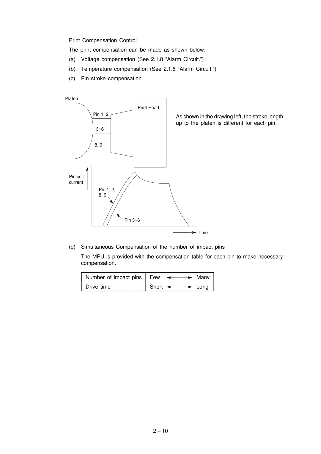
(c)Pin stroke compensation
Platen
Pin coil current
Pin 1, 2
3~6
8, 9
Pin 1, 2, 8, 9
Print Head
As shown in the drawing left, the stroke length up to the platen is different for each pin.
Pin 3~6
![]() Time
Time
(d)Simultaneous Compensation of the number of impact pins
The MPU is provided with the compensation table for each pin to make necessary compensation.
Number of impact pins | Few |
| Many |
| |||
|
|
|
|
Drive time | Short |
| Long |
| |||
|
|
|
|
2 – 10