|
|
| CH IN | + |
|
| |
~ |
|
|
|
|
|
| |
V s | Vs + V g2 - V g1 | Inp ut |
| To A /D | |||
A m p |
| ||||||
|
| LL GN D | - |
|
| ||
|
|
|
|
| |||
|
|
|
|
|
|
| |
|
|
|
|
|
|
|
|
|
|
|
|
|
|
|
|
g1
g 2
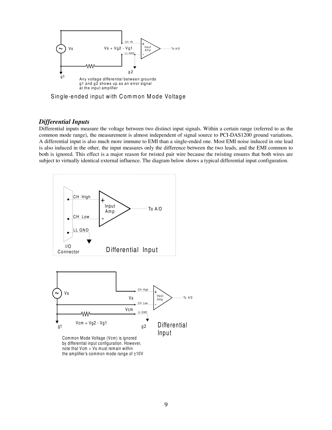
An y volta ge differential betw een grounds g1 and g2 show s up as an error signal at the input am plifier
S in gle
Differential Inputs
Differential inputs measure the voltage between two distinct input signals. Within a certain range (referred to as the common mode range), the measurement is almost independent of signal source to
CH High
CH Low
LL GN D
I/O
Connector
+
Inp ut |
| To A /D |
A m p |
| |
|
|
-
Differential Input
~ | CH High |
Vs |
+
Inp ut
Vs |
CH Low |
Vcm |
LL GND |
A m p
-
To A/D
g1 | Vcm = Vg2 - Vg1 |
g 2 |
Common Mode Voltage (Vcm) is ignored by differential input configuration. However, note that Vcm + Vs must remain within
the am plifier’s comm on mode range of ±10V
Diffe rential Inp ut
9
