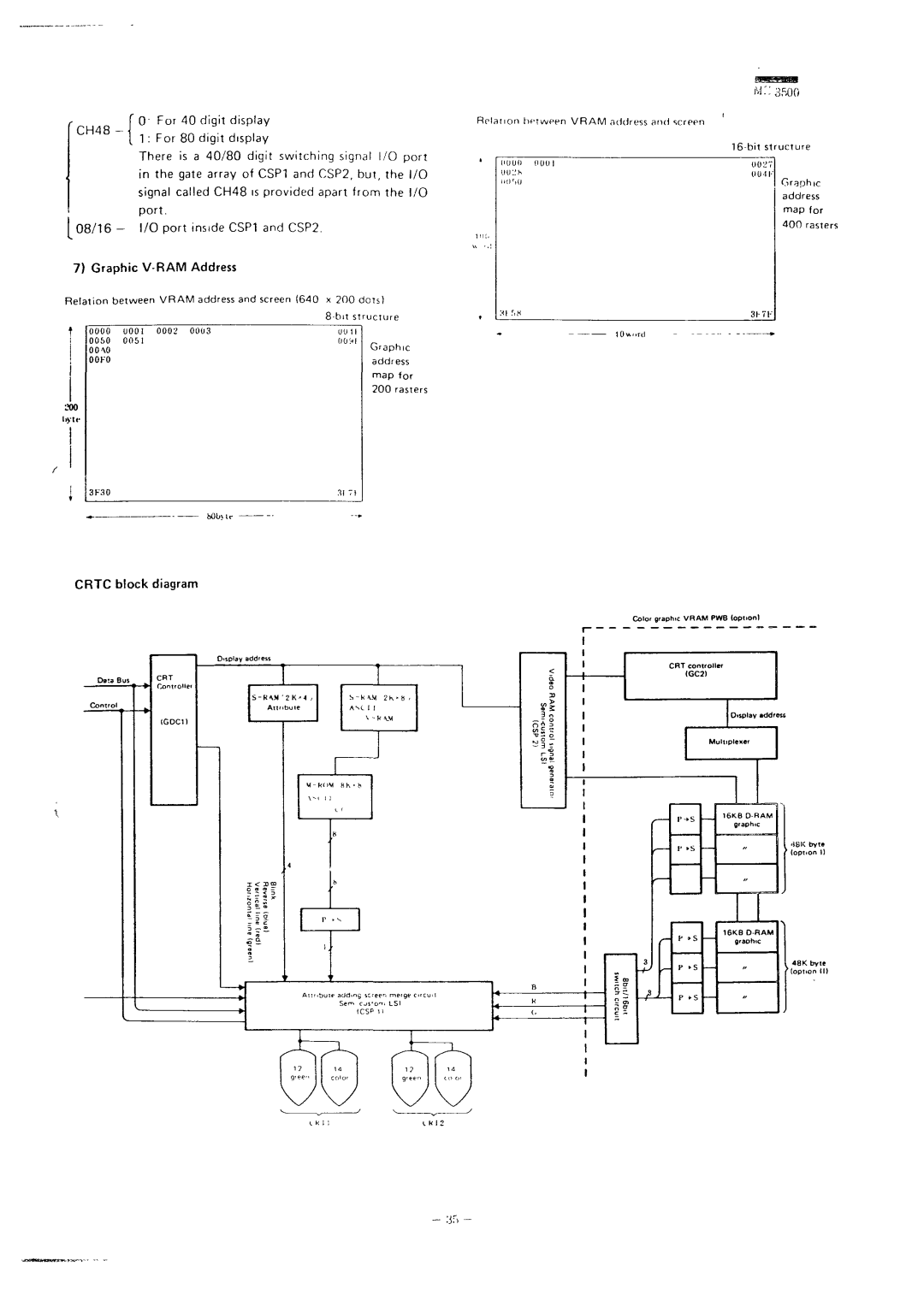
CH48 - | 0 For 40 digit display | Relation between VRAM address and screen |
1 : For 80 digit display |
| |
| ||
| There is a 40/80 digit switching signal I/O port | |
|
| |
| in the gate array of CSP1and CSP2, but, the I/O | Graphic |
| signal called CH48 is provided apart from the I/O | |
| address | |
| port. | map for |
I 08/16 - | I/O port inside CSP1and CSP2. | 400 rasters |
7) Graphic V-RAM Address
Relation between VRAM address and screen (640 x 200 dots)
| |
t lnntn0000"~^ | ~ |
0050 | Graphic |
00\0 | |
OOFO | address |
| map for |
| 200 rasters |
LXH) |
|
liytr |
|
bOb\ir —
CRTC block diagram
Color graphic VRAM PWB (option)