Personal Computer Model Z-350
Memory
Timer
BACKUP, INIT, COPY, DEBUG, Killall
Video
LSI, 1C Cmosic
Refer to the page TIN Circuit Diagram
Slot Slot2
SFDI/F
Sdisp
Preset
Symbol
Change Disp
System
Basic Area RAM
Base
User
MZ-1D07
MZ3500 System configuration of Model
Software Memory Configuration
MS1 = D MSO = 0 L
Timing of Reset Signal
SD1 System Loading & CP/M
ROM-IPL
Ffff
Bank Select
MAO
Bank
SD3 RAM based Basic
Operational description
ROM
Block diagram Relation between MMR main memory
Main Memory Mapper
This paragraph discusses main CPU I/O
Main CPU and I/O port
Table below describes address map
MZ3500
0001
Main CPU \m
Sub CPU and I/O port
Address BUS
Memory mapper MMRSP6102R-001 Block diagram
To Reset
Coab
RAS ROW Address Select Line Address Select Signal
MZ3500 Memory mapper MMR SP6102R-001 signal description
Srdy
Pin No
RO1B
IN/OUT
RO2B
D2 Dl 1 1 1 1 1 0 FE do D4 D3
A7 A6 A5A4A3A2AlAO H E X Uhus 1 O
1 1 1 1 0 KI1 Dl Do 17 D6 D5
1 1 1 1 1 1 FF 14 I N D3
MZ3500 Memory ROMIPL, RAMCOM, S-RAM select circuit
Specification
CRT
Summary of video display specification
Asci
Dot color designated by
Dot pitch
Blue
Graphic dot
KA7
CH AT
CH AI +,! AT A r + + G
#1 FFF
Ascii CG
Video RAM Structure of Vram
#07FFA
Structure of character Vram When read/write from GDC
#0000
Read/write by Z-80 via the GDC 640 x 200 dots display mode
8bit
16K
FV = 60 Hz
Master/slave setup by combination
640 x 400 bits display mode FH = 20.92 kHz FV = 47.3 Hz
Setup of GCD master/slave
O signal switching
Crtc block diagram
Graphic V-RAM Address
Page
Master slice LSI CSP-1 SP6102C 002 signal description
» CK
CSP-1 Block Diagram
CSH
LSI CSP-2 SP6012C-003 Signal Description
HSY2 2BLK2
DSP2 OUT
CSP 2 Block Diagram
3r00
CAS OUT
GDC Graphic display controller UPD7220 signal description
AT~BTI
AD15ILC2
NK-CLC
CSR-1MAGE
CG Address Select Circuit
Structure
Vsync
Circuit description
Character Vram select circuit
Blsc
Set GDC command code
Read/write from the Z-80 to V-RAM
Write C 23H Command Code Vecte C 6CH Command Code
Return when all parameters were sent
Csrw C 49H -COMMAND Code
Fifo Empty?
VECTE. Dot address is structured on the screen
60H
Explanation
Following manner Dot display program example-1
P4 88H P5 HH
I T E C 23H
Kind of line solid line
Floppy disk
Outline
TJ ILJ n
VnVn n nV nnn7
Ci D ci Ici
Data
MZ3500 MFD interface block diagram
FDC UPD765
22 «- o Window
UPD765 signal description
Port used in the MFD interface is as follows
Trigger motor on of the timer 555 Selects FDD
MZ350C
MFM recording method
3500 Precompensate Circuit
Controls during read, write, seek, and re- calibrate
Media detection
Control during seek and recalibration
VFO circuit
Purpose String of data Pulses from the FDD Data window
VFO circuit configuration
Filter Phase Detector Amplifier Window
MFM Mode
BQA
FM mode timing chart
\\\\
Aload
Side =
3DSC
Track 10 sector
76 iy 7 EH 77 / FFH
\128
Indicates the byte position From the top of directory
39 B74 B75
Ii Patat
B144 6145 B146 B147 39 B148 B149 B150 B151
1015
MZS500
General specification
Data transmission format
Example 7-bits, even parity, 1 stop bit
Start
AC controls
OFF
KTS
MZ3500 Data output control
8251 AC
3SOO
RXEN,UTR , T X E N
256
200
9 6.3
128
Wl -»
«--N
8253
8253 OUT
DAT
Printer interfacing circuit
AA3
DS7
Output
General description of the parallel interface
Data transfer timing
I/O port map
Write Hold SET
Clock circuit Schematic
Read Hold
DIN
MZ3500 PD1990AC Block diagram
LSB MSB
Mmmil
» GETE1 J
GP I/O
3500
S I C
SFD 1/F
SEC
SW2 SW1 On on CE332P OFF on MZ1P02 On OFF IO2824 OFF OFF
Dipswa
FD2
\f Canbe in either state
Functions
Block diagram
Description of each block
Switching regulator
+5V
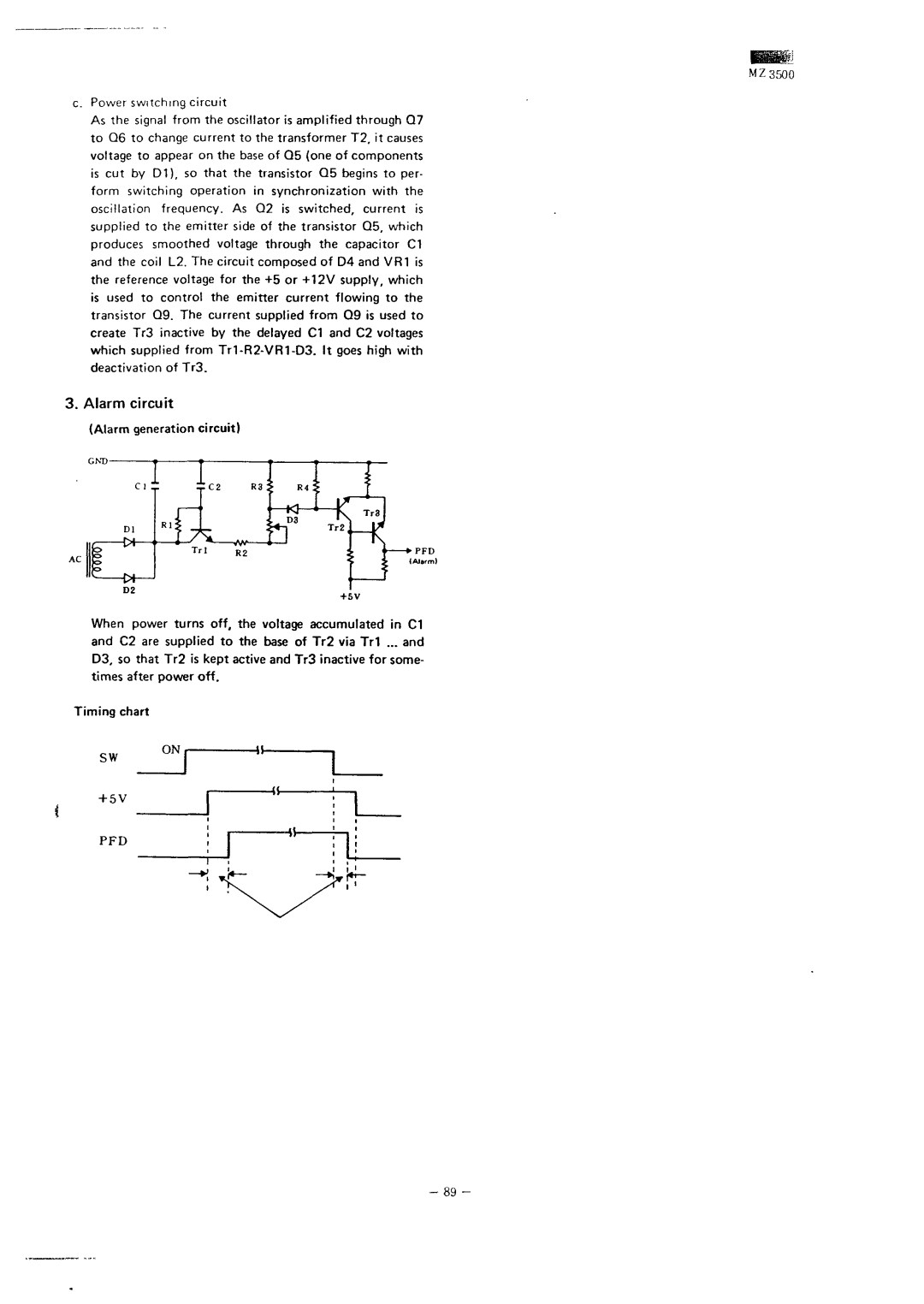
Alarm generation circuit
Timing chart
At rrn
Specification of keyboard control
Key
Key
Key search timing
2s 2s22 21
Strobe
22.5/-s
132.5
Protocol Key to sub CPU
Keyboard controller basic flow
PIN
Keyboard controller signal description
XTAL1 XTAL2 Reset INT
ALE DBO DB7 GND
On OFF
Procedure
Sub-CPU side
Abnormal
Shared RAM
CRT inter face test
S C I I 00-FF
1 5 c * O DR O.7
Abnormal test ending
Ready O.H
ROM-IPL Main CPU Checker Flow Chart 1/2
Main CPU Checker Flow Chart M?
100
101
M7*500
Keyboard controller ROM test
Keyboard test
IPL Flow Chart
Error
Jump \ Boot Address System
SEEK, Read Error
Load Iocs SEEK& Read
SUB CPU IPL Flow Chart
105
LJ LJ LJ LJ LJ LJ LJ
R R R R F1
LU LU U LJ LlJ LJ U U
U J l J J L i J L L j l J J L l J L L l
AIO
IwC
RoB
MZ-35OO Parts Guide LI
LED PWB
No Parts Code
S C R I P T I O N
IE--or Ooss-zw
N T K
MZ-3500
Parts Code
Qcnw
Connector
S C R I P T I O N
Parts Code
MZ-3500
NO. Parts Code
A a N a D
VH S N 7 4 0 6 N
NEW
Mark Rank
Part S C R I P T I O N
Coos
J9, MZ1K02,1K03,1K04,1K05 Key unit
M2-3500
LA a
SOC
LSI RAM
NO. Parts Code
D e
Tin
Parts Code
N a a
MZ-3500
Sharp Corporation