Sharp MZ-3500 service manual MZ3500 Memory ROMIPL, RAMCOM, S-RAM select circuit

Models: MZ-3500

1 116
Download 116 pages 54.05 Kb
Page 21
Image 21

MZ3500

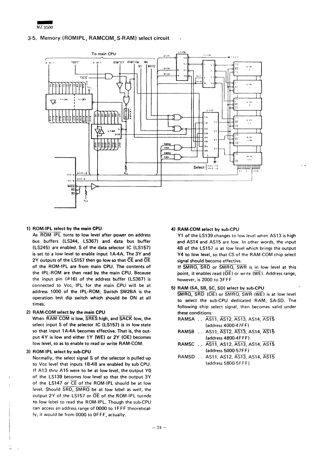
3-5. Memory (ROMIPL, RAMCOM, S-RAM) select circuit

To main CPU

1)ROM-IPL select by the main CPU

As ROM IPL turns to low level after power on address bus buffers (LS244, LS367) and data bus buffer (LS245) are enabled. S of the data selector 1C (LS157) is set to a low level to enable input 1A-4A. The 3Y and 2Y outputs of the LS157 then go low so that CE and OE of the ROM-IPL are from main CPU. The contents of the IPL-ROM are then read by the main CPU. Because the input pin (^16) of the address buffer (LS367) is connected to Vcc, IPL for the main CPU will be at address 1000 of the IPL-ROM. Switch SW2BA is the operation test dip switch which should be ON at all times.

2)RAM-COM select by the main CPU

When RAM COM is low, SRES high, and SACK low, the select input S of the selector 1C (LS157) is in low state so that input 1A-4A becomes effective. That is, the out- put 4Y is low and either 1Y (WE) or 2Y (OE) becomes low level, so asto enable to read or write RAM-COM.

3)ROM-IPL select by sub-CPU

Normally, the select signal S of the selector is pulled up to Vcc level that inputs 1B-4B are enabled by sub CPU. If A13 thru A15 were to be at low level, the output YO of the LS139 becomes low level so that the output 3Y of the LS147 or CE of the ROM-IPL should be at low level. Should SRD, SMRQ be at low lebel as well, the output 2Y of the LS157 or OE of the ROM-IPL turnde to low lebel to read the ROM-IPL. Though the sub-CPU can access an address range of 0000 to 1FFF theoretical- ly, it would be from 0000 to OFFF, actually.

4)RAM-COM select by sub-CPU

Y1 of the LS139 changes to low level when AS13 is high and AS14 and AS15 are low. In other words, the input 4B of the LS157 is at low level which brings the output Y4 to low level, so that CSof the RAM-COM chip select signal should become effective.

If SMRQ, SRD or SMRQ, SWR is in low level at this point, it enables read (OE) or write (WE). Address range, however, is 2000 to 3FFF

5)RAM (SA, SB, SC, SD) select by sub-CPU

SMRQ, SRD (Of) or SMRQ, SWR (WE) is at low level to select the sub-CPU dedicated RAM, SA-SD. Tne following chip select signal, then becomes valid under these conditions:

RAMSA .. ASVi, AS12, AS13, AS14, AST! (address 4000^17FF)

RAMSB .. AS11, AST2, AST3, AS14, AS15 (address 4800-4FFF)

RAMSC .. AS11, AS12, AS13, AS14, AS15 (address 5000-57FF)

RAMSD .. AS11, AS12, AS13, ASK, ASHi (address 5800-5FFF)

- 24 -

Page 21
Image 21
Sharp MZ-3500 service manual MZ3500 Memory ROMIPL, RAMCOM, S-RAM select circuit