Introduction
Functional Block Diagram
AN93
Table of Contents
AN93
AN93
AN93
AN93
Document Change List Contact Information
Modulations
Selection Guide
Protocols
Protocol Function Si2494/93 Si2457 Si2439/34 Si2415 Si2404
ISOmodem Capabilities
Carriers and Tones
Release
Part Numbers Package
Reset Sequence
Resetting the Device
Modem System-Side Device
Reset Strapping General Considerations
Reset-Strap Options for 16-Pin Soic Package
SOIC-16 Reset-Strap Options
Mode Reset-Strap Pins Interface Input Clock Pin 5, RXD/MISO
Reset-Strap Options for 24-Pin Tssop Package
TSSOP-24 Parallel-Interface Options
TSSOP-24 UART-Interface Options
TSSOP-24 SPI-Interface Clock-Frequency Options
Reset Strapping Options for QFN Parts with Uart Operation
Input Clk
Reset Strapping Options for QFN parts with SPI Operation
Pin Functions vs. Interface Mode TSSOP-24
Pin Functions vs. Interface Mode SOIC-16
System Interface
Pin Functions vs. Interface Mode QFN-38
SPI-Interface Signals
UART-Interface Signals
Parallel-Interface Signals
DTE Rates
Ideal DTE Rate bps Actual DTE Rate bps Approximate Error%
Symbol Data bits Parity Stop bits
Serial Formats Detected in Autobaud Mode
Flow Control
U70 Bit Function
Can Monitor
PPD
OCD
Parallel and SPI Interface Operation
Uart Serial Interface
TX Fifo
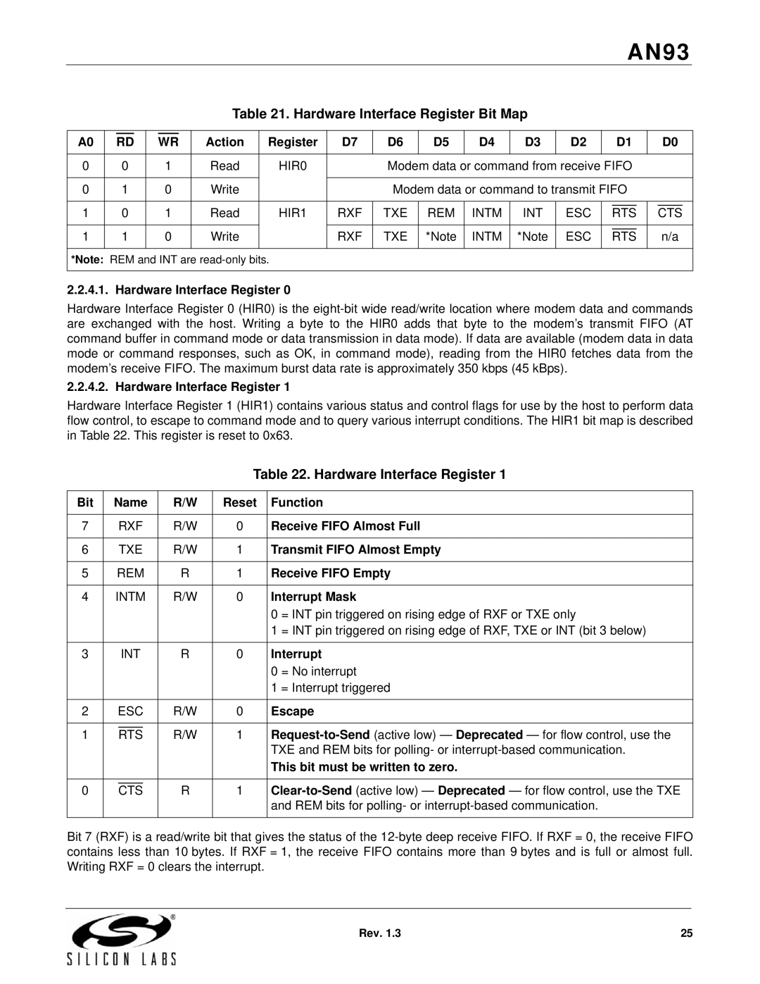
Hardware Interface Register
Hardware Interface Register Bit Map
Signal Function Direction
Parallel Interface Signals
Parallel Interface Operation
Parallel Interface Read Timing
SPI Control-and-Address Bit Definitions
Bit Function Meaning when High Meaning when Low
SPI Interface Operation
Interface Communication Modes
Power-Down Mode
Low-Power Modes
Wake-on-Ring Mode
Sleep Mode
Signal Pin Number TSSOP-24 QFN-38
SSI/Voice Mode 24-Pin Tssop and 38-Pin QFN Only
Clkout Fsync SDI SDO Reset
SSI Interface Pin Connection
Eeprom Interface 24-Pin Tssop and 38-Pin QFN Only
Eeprom Commands
Eeprom Status Register Any Other Bits are Unused
Eeprom Timing
EOZ
Parameter Symbol Min Typ Max Unit
Ecsh Eecs
Boot Commands Custom Defaults
Three-Wire SPI Interface to Eeprom
Detailed Eeprom Examples
Eeprom
Firmware Upgrades
AT Command Macros Customized AT Commands
Boot Command Example
Autoloading Firmware Upgrade Example
AT Command Macro Example
Combination Example
Command Function
Combination Example
Dec Hex Display
Ascii Chart
DAA Line-Side Device
Hookswitch and DC Termination
AC Termination
AC Termination Settings for the Si3018 Line-Side Device
Ringer Impedance and Threshold
Pulse Dialing and Spark Quenching
Typical Loop Voltage LVS Transfer Function
Loop Current Transfer Function
Ilim =
LVCS40 Condition
Billing Tone Detection
Legacy-Mode Line Voltage and Loop Current Measurement
Hookswitch and DC Termination
Power Supply and Bias Circuitry
Hardware Design Reference
Component Functions
Optional Billing-Tone Filter
Ringer Network
TIP From Line Ring DAA
Symbol Value
EMI/EMC
Si3018/10 Schematic
Schematic
Component Value Suppliers
Bill of Materials
Layout Guidelines
Reference Placement
ISOmodem Layout Check List
Layout Checklist
Layout Items Required
AN93
Module Design
Module Design and Application Considerations
Motherboard Design
Analog Output
Modem Module VCC and Reset Filter
Audio Quality
Audio Filter Response
Controller
Modem Reference Guide
Configuration Status
AT Command Set
Command Action
DSP
Multiple AT Commands on a Single Line
Command Examples
Command Result Comment
Command Result
Consecutive U-Register Writes on a Single Line
Basic AT Command Set
No Patch AT Command Chip Revision
Enable
Modifier
ATI0 ATI1
Revision B Patch rbpXYYYY
AT Command Chip Revision
Revision C Patch rcpXYYYY
ATI0
Speaker is always off
Enable result codes See Table
Command Action Verbal result codes
Program RAM write this command is used to upload firmware
+DR=X
Disabled
+DRNONE
+DRV42B RD
Connection = Disable synchronous access mode
Specifies the mode of operation when initiating a modem
Specifies the mode of operation when answer a modem
C,D
= Nrzi encoding and decoding disabled
= CRC generation checking disable
Specifies action taken if an underrun condition occurs
During transparent sub-mode
Class 1 Transmit Carrier
Country
United States default
Fixed DTE Rate
+GCI?
Automatically detect the baud rate
BPS
V32B ITU-T V.32bis default for Si2415
V22B ITU-T V.22bis default for Si2404
ITU-T V.34 default for Si2434
ITU-T V.90 default for Si2457
+PMHR=X
Enable Short Phase 1 and Short Phase
+PMHT=X
+PQC=X
= After ring only
DCEs decide to use short startup procedures
= Off
Distinctive Ring
Load Voice Factory Defaults
Command Action Transmit Gain Selection
DTE/DCE Inactivity Timer
ISOmodem on-hook. Aout disabled. Tone detec
Ringing Tone Never Appeared Timer
Ringing Tone Goes Away Timer
OK result code. Default time is 0 seconds
Is five seconds
Dtmf / Tone Duration Timer
Speakerphone AEC, AES and LEC disabled
Voice Compression Method
Signed PCM
Extended AT& Command Set
Extended AT Commands
Kbps max default for Si2415
Kbps max default for Si2457 transmit and Si2434
Only 56 kbps to 28 kbps
TIP +
Enable V.42bis in transmit and receive paths
Extended AT% Command Set
ISOmodem answers a call in answer mode
Disable automatic line-in-use detection
Mode is not allowed with a parallel or SPI interface
Extended AT\ Command Set
\Q2 Use CTS only
\P0 Even
\T16 Autobaud On4
\T9 Kbps4
\V0 Report connect and protocol message
Numeric1 Meaning Verbal Response
Result Codes
Polarity Reversal
Stas
No Polarity Reversal
Protocol None
UN-OBTAINABLE Number
ALTERNATE, +CLASS
Disconnect Code Reason
Disconnect Codes
Registers
Definition Register Function Default Range Units Decimal
Register Descriptions
Ascii
All spaces 0s
Symbol Rate Allowable Data Rates
2400 Symbols/second
Register Address Name Description Default Hex
DT4A0
U0F
DT4B1
DT4B2
Bmtt
U2E
U2F
Bdlt
Prdd
U4E
U4F
FHT
Samco
V9AGG
Sasf
SC0
Register Summary
Bit-Mapped U-Register Summary
U0-U16 Dial Tone Registers
Register Name Description Default
2. U00-U16 Dial Tone Detect Filter Registers
3. U17-U30 Busy Tone Detect Filter Registers
U17-U30 Busy Tone Detect Registers
BPF Biquad Stage Output Scalar
310/510 Default Busy and Dial Tone
300/480
320/630
400/440
BPF Biquad Values
Dial Tone Timing Register
Ringback Cadence Registers
4. U31-U33 Ringback Cadence Registers
5. U34-U35 Dial Tone Timing Register
Dtmf Dial Registers
Pulse Dial Registers
7. U46-U48 Dtmf Dial Registers
8. U49-U4C Ring Detect Registers
Ring Detect Registers
9. U4D Modem Control Register 1-MOD1
Register U4D Bit Map
Flash Hook Time Register
Pre-Dial Delay Timer Register
Loop Current Debounce Registers
Transmit Level Register
U54 Bit Map
U53 Bit Map
U62 Bit Map
U65 Bit Map
U63 Bit Map
17. U67-U6A International Configuration Registers
Line-Side Chip Power Down
PDL
= Normal operation
U67 Bit Map
U66 Bit Map
U68 Bit Map
U6C Bit Map
U6A Bit Map
18. U6C Line-Voltage Status Register
19. U6E-U7D Modem Control and Interface Registers
U6F Bit Map
U6E Bit Map
Ptmr
U70 Bit Map
Disables PCM mode Enables PCM mode
Type Reset settings = Bit
U71 IO1 Bit D15 D14 D13 D12 D11 D10 Name
Function 155 Reserved Read returns zero
U77 Bit Map
U76 Bit Map
U78 Bit Map
Monitor Mode Values
U79 Bit Map
= Normal Atdtw operation
U7A Bit Map
Adaptive Dialing
= Normal asynchronous mode
Synchronous Mode
Pin indicates valid ring signal
Given time
= Timed calibration disabled
= Disables No Loop Current Detect
= ATZ enabled
20. U80 Transmit Delay for V.22 Fast Connect
= Ignore unrecognized in-band commands
Special Error Reporting Mode
Minimal Transparency
Framed Sub-Mode Startup
Firmware Upgrades
Escape Methods
Patch, 115 kbaud Uart Lines Reset, then
Load Technique and Speed Table
Method
Th Bit Escape
1. +++ Escape
Escape Pin Escape
Wire Mode
Error Correction
Enabling Error Correction/Data Compression
To Enable Use AT Commands
15. V.80 Mode
Legacy Synchronous DCE Mode/V.80 Synchronous Access Mode
Synchronous Mode Overview
Epos Electronic Point of Sale Applications
AT\N0
Synchronous Access Mode Settings
Indicator pair Code Transparent Submode
Command Hex Supported Transmit Direction Receive Direction
CRC
EM In-Band Commands and Statuses
Command
Fast Connect Settings
Supported Transmit Direction Receive Direction
Code Transparent Submode
ATDT12345 Connect 1200 Protocol None
0x190x190x110x11
Function/Feature AT Commands Registers
Modem Feature vs. Hardware, AT Command and Register Setting
Programming Examples
Quick Reference
DC Termination Control Bits
Country-Dependent Setup
DC Termination
Reg Bit Val Function
Country Initialization Table
Country Configuration
Country Initialization Table
Country Initialization
AT+GCI=F
AT+GCI=A
AT+GCI=16
AT+GCI=9C
AT+GCI=27
AT+GCI=26
AT+GCI=31
AT+GCI=6C
AT+GCI=3D
AT+GCI=3C
AT+GCI=42
AT+GCI=53
AT+GCI=46
AT+GCI=57
AT+GCI=58
AT+GCI=0
AT+GCI=59
AT+GCI=61
AT+GCI=9F
AT+GCI=7B
AT+GCI=69
AT+GCI=82
AT+GCI=7E
AT+GCI=89
AT+GCI=87
AT+GCI=A0
AT+GCI=B8
AT+GCI=A6
AT+GCI=A5
AT+GCI=FE
UAE
AT+GCI=B4
International Call Progress Registers
Line Interface/Control Registers
Dial Registers
Special Requirements for Serbia and Montenegro
AT Command Function
Blacklisting
S42 Blacklisting
Caller ID Modes
Caller ID
SMS Support
SMS Commands
Japan Caller ID
Protocol
150
Mdmf Parameters
Type II Caller ID/SAS Detection
Character Description Hexadecimal Value Ascii Value
Johndoe
SAS Cadence for Supported Countries
SAS Tone Frequency
Aruba
Country Tone Frequency Hz Cadence seconds Registers
Australia
Austria
Croatia
Country Tone Frequency Hz Cadence seconds Registers China
Cyprus
Czech Republic
Guyana
Greece
Honduras
Hong Kong
Japan
Israel
064 0.436
Jordan
Korea Republic
Kiribati
Lao P.D.R
Lithuania
Oman
Nigeria
Papua New Guinea
Paraguay
St.-Kitts-and-Nevis
Country Tone Frequency Hz Cadence seconds Registers Russia
St. Lucia
Saudi Arabia
Tajikistan
Sweden
Trinidad
Tobago
On-Hook Condition
Intrusion/Parallel Phone Detection
Line Not Present/In Use Indication Method 1-Fixed
Loop Voltage Action
Off-Hook Condition
Line Not Present/In Use Indication Method 2-Adaptive
Register Bits Name Function
Intrusion Detection
ATH1
Modem-On-Hold
Possible Responses to Pmhr Command from Remote Modem
Initiating Modem-On-Hold
Value Description
Receiving Modem-On-Hold Requests
Hdlc Bit Errors on a Noisy Line
DCE
Bit Errors
Beginning of Packet
Data Meaning
Bit Errors
0D 0A 4E 4F 20 43 52 49 45 52 0D 0A
Pulse/Tone Dial Decision
Overcurrent Detection
Overcurrent Detection
Register Bit Value Function
Automatic Phone Line Configuration
Possible +PMHT Settings
Telephone Voting Mode
12. V.92 Quick Connect
AT+PSS Parameters
AT+PQC Parameters
Handset, TAM, and Speakerphone Operation
Extended AT+ Command Set
Software Reference
Caller ID Enable
Command Action Caller ID Type
After ring only
Distinctive Ring Cadence Reporting
Command Action Analog Source / Destination Selection
Speakerphone AEC, AES and LEC disabled. Handset FIR filter
Command Action Ringing Tone Never Appeared Timer
+VTS command. Default time is 1 second dur =
Compression Selection Method
Transmit Voice Stream
Command Action Dtmf and Tone Generation
DLE Commands DTE-to-DCE
DLE Commands DTE-to-DCE
Code Hex Simple Action Command Description
Format DLECode
DLE Events DCE-to-DTE Simple Event Reporting
DLE Simple Events DCE-to-DTE
Code Hex Description
SUB
180
Description Default
Voice Mode U Registers Address
Complex Event Reporting
Format DLEXResponseDLE Description
Register Address Name Description Default
Voice Mode U Registers
HRXFIR2
HRXFIR1
HRXFIR3
HRXFIR4
STXFIR2
STXFIR1
STXFIR3
STXFIR4
SRXFIR2
SRXFIR1
SRXFIR3
SRXFIR4
U199 Bit Definitions
U19E
Voice Reference-Overview
TAM, Handset, and Speakerphone Voice Paths
Rev 189
+VTX +VRX +VSP +VTS
Voice Mode Operations +FCLASS=8
Event +VNH = ATH or
Input Current Modem Settings Command or
DTR off &D2
ATZ or
Si3000 Configuration
TAM Pstn
System Voice Modes
Initialization Sequence
Initialization
Rev 195
Handset
Handset Configuration
Overview
AT+VLS=13
AT+VLS=0
AT+VSP=0
Handset Manual Off-Hook Dial
Handset Automatic Tone Dial
Handset Automatic Pulse Dial
Terminate
Handset to TAM Hands-Free Transition
AT+VLS=14
Speakerphone Transition
Handset to Speakerphone Transition
AT+VSP=1
Local Ring Notification with Type I CID Event
Telephone Answering Machine
NAME=JONES Jennifer
Record OGM
TAM Hands-Free Record OGM
ATU199&FFFD
AT+VRX Connect
Review OGM
TAM Hands-Free Review OGM
Record Local ICM
Review ICM
TAM Handset Record OGM
Trigger receive operation. The first byte
TAM Handset Review OGM
AT+VSM=4
Normal Answer OGM Playback with ICM Record
TAM Pstn Normal Answer OGM Playback with ICM Record
ICM
AT+VLS=15
Interrupted Answer OGM Playback with Dtmf Menu Entry
DLE1 Dtmf 1 digit detected
Simplex Speakerphone
Speakerphone
Transmit Gain Calibration-Speakerphone Disabled
Register Name Description Default Value
Simplex Speakerphone U Registers
External Microphone/Speaker Calibration
Transmit Gain Configuration
AT+FCLASS=8
Transmit/Receive Gain Calibration Dial Remote Telephone
Receive Gain Reference Measurements
Receive Gain Configuration
Reg Name Bit U19E
Speakerphone Calibration-AEC Gain Calibration
AEC Gain Calibration Dial Remote Telephone
Speakerphone Configuration
Speakerphone Configuration
Simplex Speakerphone Configuration
Speakerphone Automatic Tone Dial
Simplex Speakerphone Configuration
Speakerphone Manual Off-Hook Dial
Call-Automatic Tone Dial
Speakerphone to Handset Transition
Speakerphone Automatic Pulse Dial
Call-Automatic Pulse Dial
References
Glossary
Termination
Implementing the SIA Protocol
Security Protocols
AT+F0
Considerations when Disconnecting the Session
AT+F2
AT+F1
AT+F3
AT+F4
Result Code Meaning Remarks
Implementing the Ademco Contact ID Protocol
Dtmf Digit Low Tone Hz High Tone Hz Contact ID AT Command
Ademco Contact ID Protocol Tone Transmission AT Commands
Modem Specific Implementation Details
Kissoff
Step DTE-to-Modem Command Modem-to-DTE Remarks Indication
Ademco Mode of Operation
Handshake Tone Detection
Event Modem-to-DTE indication Remarks
Wait for Receiver to answer with handshake tones
Delay 250 ms before transmitting Data Tones
Message
ATH
Wait for Kissoff tone
Rev 233
SMS Message Format
Chinese ePOS SMS
AT Commands for SMS
SMS AT Command Set
AT Command ISOmodem Response Description
+FCLASS=256
= Auto Mode
Register Bits Name Description Default Hex
User Registers for SMS Operations
SMS User Registers
Example
Procedure
Crlfconnect Crlf
Dleetxcrlfno Carriercrlf
Response
Connect 1CRLF
Connect 2CRLF
Dleetxcrlfokcrlf
Example Session
POS
SMS Process in Host and Modem
Prototype Bring-Up Si3018/10
Testing and Diagnostics
Command Timing
Inappropriate Commands
Register Configurations
Host Interface Troubleshooting
10.1.6. Si3018/10 Troubleshooting
Isolation Capacitor Troubleshooting
Component Troubleshooting
Connect Evaluation Board to Prototype System
EVB
Test the Host Interface
Test the Prototype Si3018/10 Circuitry
Si3018/10 Resistance
Si3018/10 Typical Voltages Resistance to Si3018/10 Pin
Voltages across Components with Diode Checker
Resistance across Components
FB1 FB2 RV1
Component Voltage
Loop Test Circuit
Self Test
Bell 103-V.34 Modem Functional Test Connection
Board Test
Isdn Modem
Teltone ILS
Modem Under Test
Test Coverage
AT Commands for Compliance Testing
Compliance Testing
AT Command/Test Method Desired Response
S41 Symbol Rate Allowable Data Rates
Symbol/Data Rate
29 Data Rate
Transmit Modulation Data Rate
Surges
Safety
Published Coilcraft TRF-RJ11 Filter Performance
AM-Band Interference
Debugging the DTE Interface
Debugging the DTE interface
Modulation
Appendix A-EPOS Applications
Recommendation
0xFF 0x19 0xA0 0x19 0xB1
ISOmodem V.80 Protocol Hdlc Framing in Framed Sub-Mode
ISOmodem in Epos Applications
29 FastPOS Sample Program
Setup procedure
AT&D2
AT+FCLASS=1
Example Program in C/C++
How to use the program
Rev 263
264
Rev 265
True
Rev 267
= Rtscontrolenable
Rev 269
270
FastPOS Detailed Wave Files
RTS not RTS signal
FastPOS DTE Trace
Times When Audio Recording May Not Help
When to Use Audio Recording
Hardware Setup
Larger of the two jacks 3.5 mm carries audio to the PC
Setting PC Microphone Input for Recording Windows NT
Sounds and Multimedia Properties
Setting PC Microphone Input for Recording Windows
Multimedia Properties
Setting PC Microphone Input for Recording Windows XP
Sounds and Audio Devices Properties
Sound Recorder
Making the Recording with Adobe Audition or WaveSurfer
Adobe Audition Temporal View of a Good V.22 Transaction
Audio Playback and Analysis
Adobe Audition Spectral View of a Good V.22 Transaction
Band Spectral Display
Recording Made at Excessive Level
Audio-Recording Pitfalls
Appearance of Bell 212 Protocol
Details of Some Low-Speed Protocols
Appearance of V.22 bis Protocol
Appearance of V.29 FastPOS Protocol
Examples of Epos Server Misbehavior
Example of Epos Server Misbehavior
Dtmf Distorted by Low Line Level
Examples of Line Impairments
Power Line Related Noise
Appendix C-PARALLEL/SPI Interface Software Implementation
MCU
Interrupt Service and Polling Layer
Hardware Access Layer
Software Description
MCUhardware.c modemhardware.c
Polling HIR1 Method
Interrupt Service Routine ISR Method
RXF Interrupt Receive Fifo Almost Full
TXE Interrupt Transmit Fifo Almost Empty
Timer Interrupt Receive Fifo Not Empty
U70 Interrupt
Parallel- or SPI-Port Interrupt-Service Flowchart
Buffer Management
Buffer Management, Status and Control Layer
Circular-Buffer Flowchart
Status and Control
Application Layer Sample Application
Modem Operation
Compiler Option Dot Commands
Making a Connection
Data Bursts
Sfrpagesave = Sfrpage
Modem Interrupt Service Sample Code
Rev 301
302
Revision 0.6 to Revision
Revision 0.5 to Revision
Revision 0.7 to Revision
Revision 0.8 to Revision
Contact Information