Chapter 1: Introduction
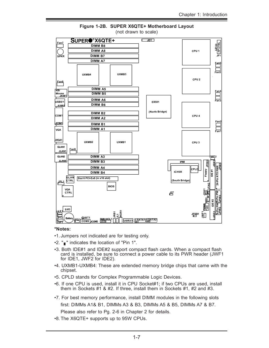
Figure 1-2B. SUPER X6QTE+ Motherboard Layout
(not drawn to scale)
|
|
|
|
| SUPER | ® |
|
|
|
| |
| Fan7 | X6QTE+ |
|
| |||||||
|
|
|
|
|
|
| DIMM B8 |
|
| ||
|
|
|
|
|
|
|
|
|
|
| |
|
|
|
|
|
|
| DIMM A8 |
|
| ||
|
|
|
|
|
|
|
|
| |||
| SPKR |
|
| DIMM B7 |
|
| |||||
|
|
|
|
|
|
|
|
|
|
| |
|
|
|
|
|
|
| DIMM A7 |
|
| ||
|
|
|
|
|
|
|
|
|
|
|
|
|
|
|
|
|
| UXMB4 |
|
| UXMB3 |
| |
| Fan8 |
|
|
|
|
|
|
| |||
|
|
|
|
|
|
|
|
|
|
|
|
|
|
|
|
|
|
|
|
|
|
|
|
|
|
|
|
|
|
| DIMM A5 |
|
| ||
| KB/ |
|
|
|
|
| |||||
|
|
|
|
|
|
|
|
|
| ||
| Mouse |
|
|
| DIMM B5 |
|
| ||||
| JKM1 |
|
|
|
|
|
|
|
| ||
|
|
|
|
|
|
|
|
| |||
USB0/1 |
|
|
|
| DIMM A6 |
|
| ||||
|
|
|
|
|
|
|
|
| |||
| JUSB1 |
|
|
|
| DIMM B6 |
|
| |||
|
|
|
|
|
|
|
|
|
|
| |
COM1 |
|
|
|
|
| DIMM B2 |
|
| |||
|
|
|
|
|
|
|
|
|
| ||
|
|
|
|
|
|
| DIMM A2 |
|
| ||
JCOM1 |
|
|
|
|
|
|
|
|
|
| |
|
|
|
|
| DIMM B1 |
|
| ||||
|
|
|
|
|
|
|
|
| |||
| VGA |
|
| DIMM A1 |
|
| |||||
JD1
E8501
(North Bridge)
CPU 1
CPU 2
CPU 4
|
| CTRL | |
|
| ||
LE1 | |||
FP | |||
|
| ||
|
|
| |
| JF1 | ||
Fan6 | |||
|
|
| |
|
|
| |
|
|
| |
Fan5 | |||
Fan4 | |||
|
|
| |
|
|
| |
|
|
| |
Fan3 | |||
Fan2
Fan1
JVGA1 | UXMB2 |
| UXMB1 | |||||
|
|
|
|
|
|
| ||
|
| GLAN1 | Fan9 |
|
|
| ||
|
| JLAN1 |
|
|
| |||
|
|
|
|
|
|
| ||
|
|
|
|
|
|
|
|
|
CPU 3
|
|
|
|
|
|
|
|
|
|
|
|
|
|
|
|
|
|
|
|
|
|
|
|
|
|
| GLAN2 |
|
|
|
|
|
|
| DIMM A3 |
|
|
|
|
|
|
|
|
|
| ||||||
|
| JLAN8 |
|
|
|
|
|
|
|
|
|
|
|
|
|
|
|
| |||||||
|
|
|
|
|
| DIMM B3 |
|
|
|
|
|
|
|
|
|
| |||||||||
|
|
|
|
|
|
|
|
|
|
|
|
|
|
|
|
|
|
|
|
|
| ||||
|
|
|
|
|
|
|
|
|
|
|
|
|
|
|
|
|
|
|
|
|
|
|
| ||
|
|
|
|
|
|
|
|
|
|
|
| DIMM A4 |
|
|
|
|
|
|
|
|
|
| |||
|
|
|
|
|
|
|
|
|
|
|
|
|
|
|
|
|
|
|
|
|
|
|
| ||
|
|
|
|
|
|
|
|
|
|
|
| DIMM B4 |
|
|
|
|
|
|
|
|
|
| |||
|
|
|
|
|
|
|
|
|
|
|
|
|
|
|
|
|
|
|
|
|
|
|
|
|
|
|
|
|
|
|
| GLAN |
| Slot 6 |
|
|
|
|
|
|
|
|
|
| |||||||
|
|
|
|
|
| CTRL |
|
|
|
|
|
|
|
|
|
|
| ||||||||
|
| JPL1 |
|
|
|
|
|
|
|
|
|
|
|
|
|
|
|
|
|
| |||||
|
|
|
|
|
|
|
|
|
|
|
|
|
|
|
|
|
|
|
| ||||||
|
|
|
|
|
|
|
|
|
|
|
|
|
|
| BIOS |
|
|
|
|
|
|
|
|
|
|
|
|
|
|
|
|
|
|
|
|
|
|
|
|
|
|
|
|
|
|
|
|
|
|
| |
|
|
|
|
| VGA |
|
|
|
|
|
|
|
|
|
|
|
|
|
|
|
| ||||
|
|
|
|
|
|
|
|
|
|
|
|
|
|
|
|
|
|
|
|
|
| ||||
|
|
|
|
| CTRL |
|
|
|
|
|
|
|
|
|
|
|
|
|
|
|
|
| |||
|
|
|
|
|
|
|
|
|
|
|
|
|
|
|
|
|
|
|
|
|
|
|
|
|
|
|
|
|
|
|
|
|
|
|
|
|
|
|
|
|
|
|
|
|
|
|
|
|
|
|
|
| JAR1 |
|
| S I/O |
|
|
|
|
|
|
| JRB1 | JL1 | WOR1 |
|
|
|
| |||||||
|
|
|
|
|
|
|
|
|
|
|
|
|
|
|
|
| |||||||||
|
|
|
|
|
|
|
|
|
|
|
|
|
|
|
|
|
|
|
|
|
|
| |||
| JP13 | Battery | JPG1 | JBT1 |
| SMB | WOL1 |
|
|
|
|
|
|
|
|
|
| ||||||||
|
|
|
|
|
|
|
|
| COM2 |
| J22 |
|
|
|
|
|
| USB2/3 |
|
| |||||
|
|
|
|
|
|
|
|
|
|
| JCOM2 |
|
|
|
|
|
|
|
|
| JS2 |
| |||
|
|
|
|
|
|
|
|
|
|
|
|
|
|
|
|
|
|
|
|
|
| ||||
| J3P1 |
|
|
|
|
|
|
|
|
|
|
|
|
|
|
|
|
| JS1 |
|
| ||||
IPMI
CPLD ICH5R
(South Bridge)
J27
JFSB1
|
|
|
|
| JWF2 | ||
|
|
|
|
|
|
| |
|
|
| JFDD1 | JIDE1 | PWR | ||
|
|
| |||||
| Floppy | IDE | |||||
|
|
|
|
| #1 | ||
|
|
|
|
|
| ||
JOH1 |
| JTAG |
| ||||
| JP2 |
| |||||
| |||||||
|
| ||||||
WD1 | #2 | ||||||
|
| ||||||
| PSSMB |
|
|
| IDE | ||
|
|
|
| ||||
|
|
|
|
| |||
JWF1 |
| I2C | JIDE2 | ||||
|
| ||||||
|
|
|
|
| |||
|
|
|
|
| |||
|
|
|
|
|
|
| |
JPW1
JPW2JPW3![]()
*Notes:
•1. Jumpers not indicated are for testing only.
•2. " ![]()
![]() " indicates the location of "Pin 1".
" indicates the location of "Pin 1".
•3. Both IDE#1 and IDE#2 support compact fl ash cards. When a compact fl ash card is installed, be sure to connect a power cable to its PWR header (JWF1 for IDE1, JWF2 for IDE2).
•4.
•5. CPLD stands for Complex Programmable Logic Devices.
•6. If one CPU is used, install it in CPU Socket#1; if two CPUs are used, install them in Sockets #1 & #2. If three, install them in Sockets #1, #2 and #3.
•7. For best memory performance, install DIMM modules in the following slots
first: DIMMs A1& B1, DIMMs A3 & B3, DIMMs A5 & B5, DIMMs A7 & B7. Please also refer to Pg.
•8. The X6QTE+ supports up to 95W CPUs.