Chapter 2: Installation
C. Front Control Panel Pin Definitions
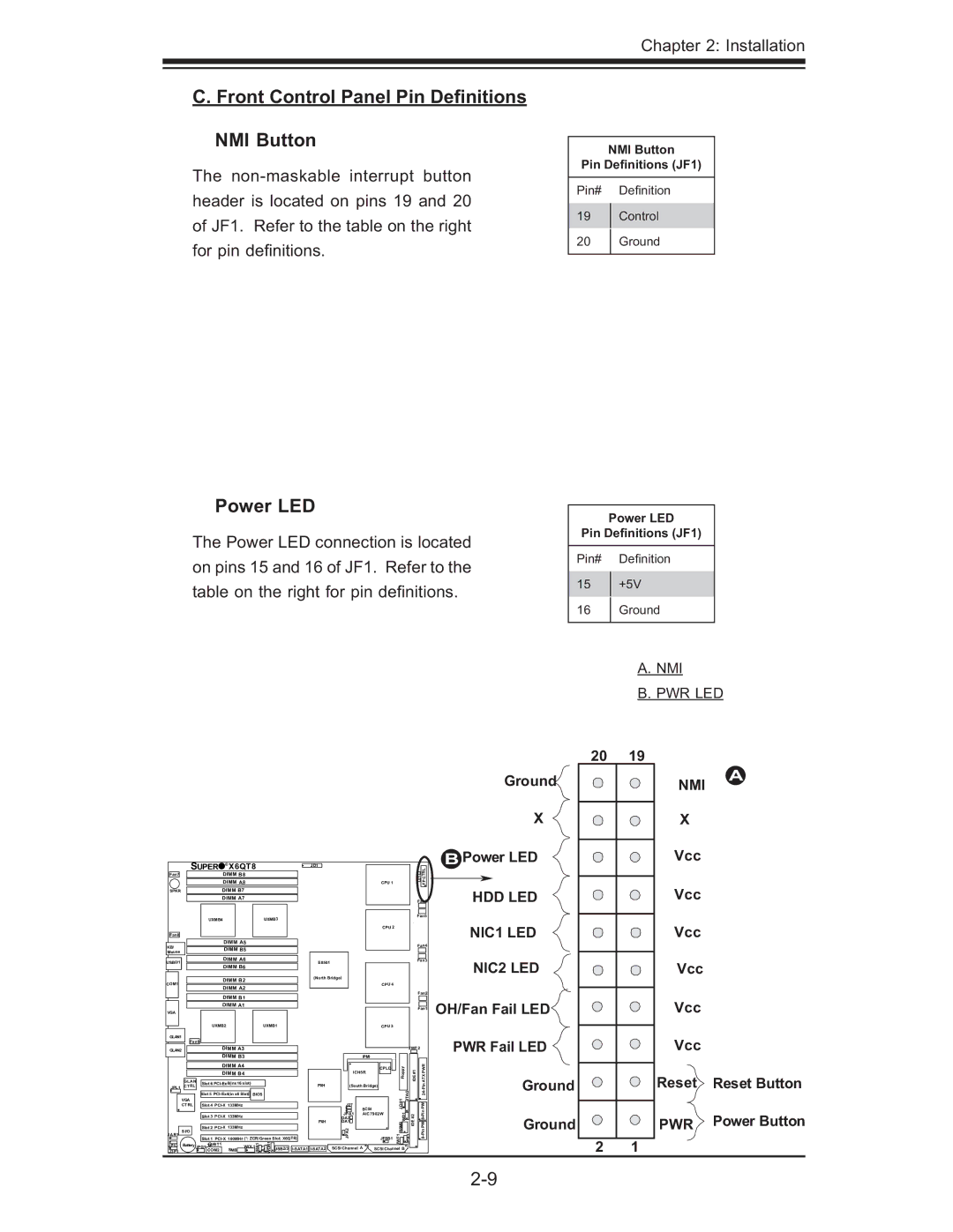
NMI Button
The
Power LED
The Power LED connection is located on pins 15 and 16 of JF1. Refer to the table on the right for pin defi nitions.
NMI Button
Pin Definitions (JF1)
Pin# Defi nition
19Control
20Ground
Power LED
Pin Definitions (JF1)
Pin# Defi nition
15+5V
16Ground
A.NMI
B.PWR LED
| SUPER | ® | X6QT8 |
|
| JD1 |
|
|
|
|
|
| CTRL | |||||
|
|
|
|
|
|
|
|
|
|
| ||||||||
Fan7 |
|
|
| DIMM B8 |
|
|
|
|
|
|
|
|
|
| LE1 | |||
|
|
|
| DIMM A8 |
|
|
|
|
|
|
| CPU 1 |
|
| FP | |||
|
|
|
|
|
|
|
|
|
|
|
|
|
| |||||
SPKR |
|
|
| DIMM B7 |
|
|
|
|
|
|
|
|
|
|
|
| ||
|
|
|
| DIMM A7 |
|
|
|
|
|
|
|
|
|
| Fan6 | |||
|
|
|
|
|
|
|
|
|
|
|
|
|
|
|
|
| ||
|
|
| UXMB4 |
|
|
|
| UXMB3 |
|
|
|
|
|
|
| Fan5 | ||
|
|
|
|
|
|
|
|
|
|
|
|
|
|
|
| |||
|
|
|
|
|
|
|
|
|
|
|
|
|
| CPU 2 |
|
|
|
|
Fan8 |
|
|
|
|
|
|
|
|
|
|
|
|
|
|
|
|
|
|
KB/ |
|
|
| DIMM A5 |
|
|
|
|
|
|
|
|
|
| Fan4 | |||
|
|
| DIMM B5 |
|
|
|
|
|
|
|
|
|
| |||||
Mouse |
|
|
|
|
|
|
|
|
|
|
|
|
|
|
| |||
|
|
|
|
|
|
|
|
|
|
|
|
|
|
|
|
|
| |
USB0/1 |
|
|
| DIMM | A6 |
|
|
|
| E8501 |
|
|
|
|
| Fan3 | ||
|
|
| DIMM B6 |
|
|
|
|
|
|
|
|
|
|
| ||||
|
|
|
|
|
|
|
|
|
|
|
|
|
|
|
| |||
|
|
|
| DIMM B2 |
|
|
|
| (North Bridge) |
|
|
|
|
|
| |||
COM1 |
|
|
|
|
|
|
|
|
|
| CPU 4 |
|
|
|
| |||
|
|
| DIMM A2 |
|
|
|
|
|
|
|
|
|
|
| ||||
|
|
|
|
|
|
|
|
|
|
|
|
|
| Fan2 | ||||
|
|
|
| DIMM B1 |
|
|
|
|
|
|
|
|
|
| ||||
|
|
|
|
|
|
|
|
|
|
|
|
|
|
|
| |||
|
|
|
| DIMM A1 |
|
|
|
|
|
|
|
|
|
| Fan1 | |||
VGA |
|
|
|
|
|
|
|
|
|
|
|
|
|
|
|
| ||
|
|
|
|
|
|
|
|
|
|
|
|
|
|
|
|
|
| |
|
|
| UXMB2 |
|
|
|
| UXMB1 |
|
|
|
| CPU 3 |
|
|
|
| |
GLAN1 |
|
|
|
|
|
|
|
|
|
|
|
|
|
|
|
|
|
|
| Fan9 |
|
|
|
|
|
|
|
|
|
|
|
|
|
|
|
| |
GLAN2 |
|
|
| DIMM | A3 |
|
|
|
|
|
|
|
|
| JWF2 |
| ||
|
|
|
| DIMM B3 |
|
|
|
|
|
| IPMI |
|
|
|
|
| ||
|
|
|
| DIMM A4 |
|
|
|
|
|
|
| CPLD | y |
|
| PWR | ||
|
|
|
| DIMM B4 |
|
|
|
|
| ICH5R |
| Flopp | #1 |
| ||||
|
|
|
|
|
|
|
|
|
|
| ATX | |||||||
| GLAN |
|
|
|
|
|
|
|
|
|
|
|
| IDE |
| |||
JPL1 | CTRL |
| Slot 6 |
|
|
|
| PXH | (South Bridge) |
|
|
| ||||||
|
|
|
|
|
|
|
|
|
| JTAG |
| |||||||
|
|
| Slot 5 | BIOS |
|
|
|
|
|
|
| |||||||
| VGA |
|
|
|
|
|
|
|
|
|
| J27 |
|
| JOH1 |
| PW | |
| CTRL |
| Slot 4 |
|
|
|
|
| SCSI |
|
| |||||||
|
|
|
|
|
|
|
|
|
|
|
|
|
|
| ||||
|
|
| Slot 3 |
|
|
|
|
| JPA1 | AIC7902W | D1W | #2 |
| 8Pin- | ||||
|
|
|
|
|
|
| PXH | DA2 |
|
|
| |||||||
|
|
|
|
|
|
|
|
|
|
| DA1 |
|
| PSSMB | IDE |
| PW | |
|
|
| Slot 2 |
|
|
|
|
|
|
|
|
| ||||||
|
|
|
|
|
|
|
| JPA2 |
|
|
|
| ||||||
JAR1 | S I/O |
|
|
|
|
|
|
|
|
|
|
|
|
|
| |||
|
| Slot 1 |
|
| JFSB1 | F1 | JPA3 |
| ||||||||||
|
|
|
|
|
| |||||||||||||
JP13 | Battery |
| JBT1 |
|
| WOL1 | JRB1 | JL1 WOR1 USB2/3 |
|
|
|
|
| JW |
| |||
JPG1 |
| SMB | SCSI Channel A | SCSI Channel B |
| |||||||||||||
J3P1 |
|
| COM2 |
|
|
|
| |||||||||||
Ground
X
BPower LED
HDD LED
NIC1 LED
NIC2 LED
OH/Fan Fail LED
PWR Fail LED
Ground
Ground
20 | 19 |
| NMI |
| X |
| Vcc |
| Vcc |
| Vcc |
| Vcc |
| Vcc |
| Vcc |
| Reset |
| PWR |
2 | 1 |
A
Reset Button
Power Button