![]()
![]()
![]() X6QT8/X6QTE+ User's Manual
X6QT8/X6QTE+ User's Manual
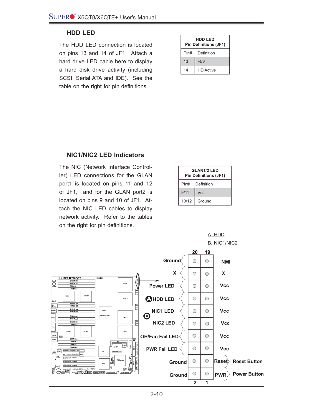
HDD LED
The HDD LED connection is located on pins 13 and 14 of JF1. Attach a hard drive LED cable here to display a hard disk drive activity (including SCSI, Serial ATA and IDE). See the table on the right for pin defi nitions.
NIC1/NIC2 LED Indicators
The NIC (Network Interface Control- ler) LED connections for the GLAN port1 is located on pins 11 and 12 of JF1, and for the GLAN port2 is located on pins 9 and 10 of JF1. At- tach the NIC LED cables to display network activity. Refer to the tables on the right for pin defi nitions.
HDD LED
Pin Definitions (JF1)
Pin# Defi nition
13+5V
14HD Active
GLAN1/2 LED
Pin Definitions (JF1)
Pin# | Defi nition |
9/11 | Vcc |
|
|
10/12 Ground
A. HDD
B. NIC1/NIC2
|
|
|
|
| SUPER | ® | X6QT8 |
|
| |||
| Fan7 |
|
|
|
| DIMM B8 |
|
| ||||
|
|
|
|
|
|
| DIMM A8 |
|
| |||
|
|
|
|
|
|
|
| |||||
| SPKR |
| DIMM B7 |
|
| |||||||
|
|
|
|
|
|
| DIMM A7 |
|
| |||
|
|
|
|
|
|
|
|
|
|
|
|
|
|
|
|
|
|
| UXMB4 |
|
|
| UXMB3 |
| |
|
|
|
|
|
|
|
|
|
|
| ||
| Fan8 |
|
|
|
|
|
|
|
| |||
|
|
|
|
|
|
|
|
|
|
|
|
|
| KB/ |
|
|
| DIMM A5 |
|
| |||||
|
|
|
| DIMM B5 |
|
| ||||||
| Mouse |
|
|
|
|
| ||||||
|
|
|
|
|
|
|
|
|
|
|
|
|
USB0/1 |
|
|
| DIMM A6 |
|
| ||||||
|
|
| DIMM B6 |
|
| |||||||
|
|
|
|
|
|
|
|
| ||||
COM1 |
|
|
|
|
| DIMM B2 |
|
| ||||
|
|
|
|
| DIMM A2 |
|
| |||||
|
|
|
|
|
|
|
|
| ||||
|
|
|
|
|
|
|
|
|
|
| ||
|
|
|
|
|
|
| DIMM B1 |
|
| |||
|
|
|
|
|
|
| DIMM A1 |
|
| |||
JD1
E8501
(North Bridge)
CPU 1
CPU 2
CPU 4
LE1 | CTRL |
| |
FP |
| ||
|
|
| |
Fan6 | |||
Fan5 | |||
Fan4 | |||
|
|
|
|
|
|
|
|
Fan3 | |||
Fan2 | |||
|
|
|
|
|
|
|
|
Ground
X
Power LED
AHDD LED
NIC1 LED
B
NIC2 LED
20 | 19 |
| NMI |
| X |
| Vcc |
Vcc
Vcc
Vcc
VGA |
|
|
|
|
|
|
|
|
|
|
|
|
|
|
|
| ||
|
|
|
|
|
|
|
| UXMB2 |
|
|
| UXMB1 |
|
| ||||
|
|
|
|
|
|
|
|
|
|
|
|
| ||||||
GLAN1 |
|
|
|
|
|
|
|
|
|
|
|
|
|
|
|
| ||
|
|
|
|
| Fan9 |
|
|
|
|
|
|
|
|
|
|
|
| |
GLAN2 |
|
|
|
|
|
| DIMM | A3 |
|
|
|
|
|
|
| |||
|
|
|
|
|
|
|
|
| DIMM B3 |
|
|
|
|
|
|
| ||
|
|
|
|
|
|
|
|
|
|
|
|
|
|
|
| |||
|
|
|
|
|
|
|
|
|
|
|
|
|
|
|
|
|
| |
|
|
|
|
|
|
|
|
| DIMM A4 |
|
|
|
|
|
|
| ||
|
|
|
|
|
|
|
|
| DIMM B4 |
|
|
|
|
|
|
| ||
|
|
|
|
|
|
|
|
|
|
|
|
|
|
|
|
|
|
|
|
|
|
| GLAN |
| Slot 6 |
|
|
|
|
|
|
| |||||
| JPL1 |
| CTRL |
|
|
|
|
|
|
|
| |||||||
|
|
|
|
|
|
|
|
|
|
|
|
|
|
| ||||
|
|
| VGA |
| Slot 5 |
| BIOS |
|
|
|
|
| ||||||
|
|
|
|
|
|
|
|
|
|
|
|
|
|
|
| |||
|
|
|
|
|
|
|
|
|
|
|
|
|
|
|
| |||
|
|
| CTRL |
| Slot 4 |
|
|
|
|
|
|
| ||||||
|
|
|
|
|
|
|
|
|
|
|
|
|
|
|
|
|
|
|
|
|
|
|
|
|
| Slot 3 |
|
|
|
|
|
|
| ||||
|
|
|
|
|
|
|
|
|
|
|
|
|
|
|
| |||
JAR1 | S I/O |
| Slot 2 |
|
|
|
|
|
|
| ||||||||
|
|
|
|
|
|
|
|
|
|
|
|
| ||||||
|
|
|
|
|
|
| Slot 1 |
| ||||||||||
|
|
| Battery |
|
| JBT1 |
|
|
| JRB1 |
| WOR1 |
|
|
|
| ||
JP13 |
| JPG1 |
|
| WOL1 | JL1 |
|
|
|
| ||||||||
|
|
|
|
|
|
|
| COM2 | SMB |
|
|
| USB2/3 | |||||
J3P1 |
|
|
|
|
|
|
|
| ||||||||||
Fan1
CPU 3
|
|
|
|
|
|
|
|
|
|
|
|
|
|
|
|
|
| JWF2 |
|
|
|
|
|
|
|
|
|
|
|
|
|
|
|
|
|
|
|
|
|
|
|
|
|
|
| IPMI |
|
|
|
|
|
|
|
|
|
|
|
| |
|
|
|
|
| ICH5R |
|
|
|
|
| Floppy |
|
| #1 | PWR | ||||
|
|
|
|
|
|
|
|
| CPLD |
|
|
|
|
|
|
|
|
| |
|
|
|
|
|
|
|
|
|
|
|
|
|
|
|
|
|
| IDE | ATX |
PXH |
|
|
| (South Bridge) |
|
|
|
|
|
|
|
|
|
| |||||
|
|
|
|
|
|
|
|
|
|
|
|
|
|
|
| JTAG |
|
|
|
|
|
| J27 | SCSI |
|
|
|
| JOH1 |
|
|
|
|
| PW | ||||
|
|
|
|
|
|
|
|
|
|
|
|
|
|
|
|
| |||
|
|
|
|
|
|
|
|
|
|
|
|
|
| D1W |
|
| #2 | ||
|
|
| DA2 |
|
|
|
|
|
|
|
|
|
| ||||||
|
|
| JPA1 | AIC7902W |
|
|
|
|
|
|
|
|
| ||||||
PXH |
|
| DA1 |
|
|
|
|
|
|
|
|
|
|
|
| IDE |
| ||
|
|
| JPA2 |
|
|
|
|
|
|
| PSSMB |
|
|
|
|
| PW | ||
|
|
|
|
|
|
|
|
|
|
|
|
|
|
| |||||
|
|
|
|
|
| JFSB1 | F1JW |
|
| JPA3 |
| ||||||||
|
|
|
|
|
|
|
|
|
|
|
|
|
|
|
|
| |||
| SCSI Channel A |
| SCSI Channel B |
|
|
|
| ||||||||||||
|
|
|
|
|
|
|
|
|
|
|
|
|
|
|
|
|
|
|
|
OH/Fan Fail LED
PWR Fail LED
Ground
Ground
Vcc
Vcc
Reset Reset Button
PWR Power Button
2 1