![]()
![]()
![]() X6QT8/X6QTE+ User's Manual
X6QT8/X6QTE+ User's Manual
VGA Connector
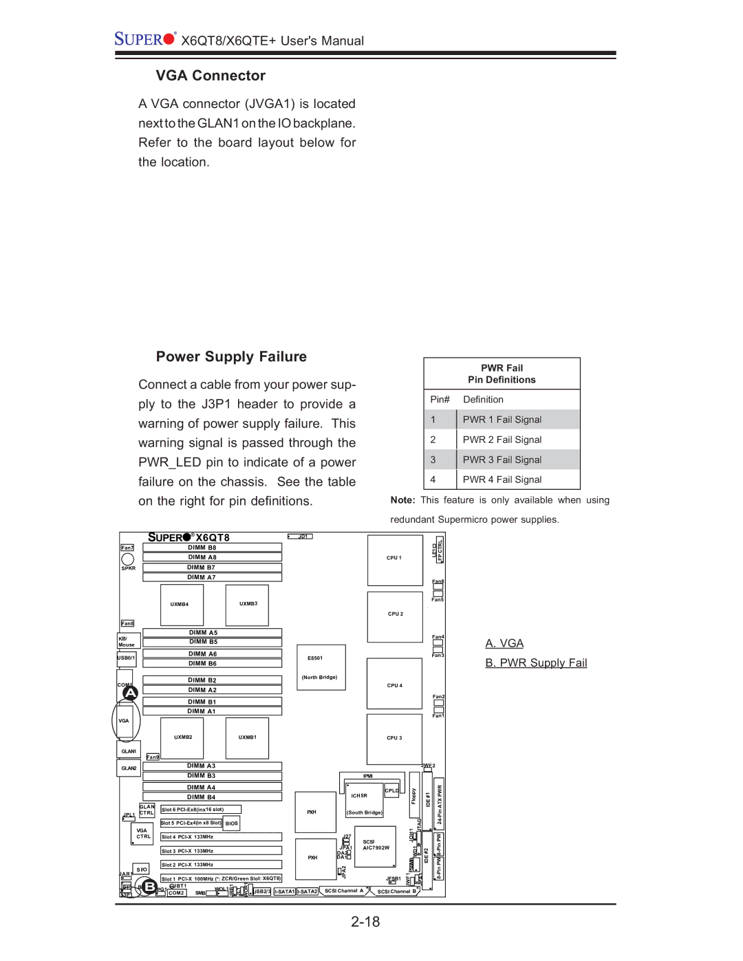
A VGA connector (JVGA1) is located next to the GLAN1 on the IO backplane. Refer to the board layout below for the location.
Power Supply Failure
Connect a cable from your power sup- ply to the J3P1 header to provide a warning of power supply failure. This warning signal is passed through the PWR_LED pin to indicate of a power failure on the chassis. See the table on the right for pin defi nitions.
PWR Fail
Pin Definitions
Pin# Defi nition
1PWR 1 Fail Signal
2 PWR 2 Fail Signal
3 PWR 3 Fail Signal
4 PWR 4 Fail Signal
Note: This feature is only available when using redundant Supermicro power supplies.
|
|
|
| SUPER | ® | X6QT8 |
|
| |||
|
|
|
|
|
|
| |||||
| Fan7 |
|
|
| DIMM B8 |
|
| ||||
|
|
|
|
|
| DIMM A8 |
|
| |||
|
|
|
|
|
|
| |||||
| SPKR |
| DIMM B7 |
|
| ||||||
|
|
|
|
|
| DIMM A7 |
|
| |||
|
|
|
|
|
|
|
|
|
|
|
|
|
|
|
|
| UXMB4 |
|
|
| UXMB3 |
| |
|
|
|
|
|
|
|
|
|
| ||
| Fan8 |
|
|
|
|
|
|
|
| ||
|
|
|
|
|
|
|
|
|
|
|
|
| KB/ |
|
|
| DIMM A5 |
|
| ||||
|
|
|
|
|
|
|
|
|
| ||
| Mouse |
|
|
| DIMM B5 |
|
| ||||
|
|
|
|
|
|
|
|
|
|
|
|
USB0/1 |
|
|
| DIMM A6 |
|
| |||||
|
|
|
|
|
|
|
|
| |||
|
|
|
|
|
| DIMM B6 |
|
| |||
|
|
|
|
|
|
|
|
|
| ||
COM1 |
|
|
|
| DIMM B2 |
|
| ||||
|
|
|
|
|
|
|
|
|
| ||
| A |
|
| DIMM A2 |
|
| |||||
|
|
|
|
|
|
|
| ||||
|
|
|
|
|
| DIMM B1 |
|
| |||
|
|
|
|
|
| DIMM A1 |
|
| |||
|
|
|
|
|
|
|
|
|
| ||
| VGA |
|
|
|
|
|
| ||||
JD1
E8501
(North Bridge)
CPU 1
CPU 2
CPU 4
LE1 | CTRL | |
FP | ||
|
Fan6
Fan5
Fan4
Fan3
Fan2
Fan1
A.VGA
B.PWR Supply Fail
UXMB2 | UXMB1 | CPU 3 |
GLAN1
Fan9
| GLAN2 |
|
|
|
|
|
|
|
|
|
| DIMM |
| A3 |
|
|
|
|
|
|
|
|
|
|
|
| |||||
|
|
|
|
|
|
|
|
|
|
|
|
|
|
|
|
|
|
|
|
|
|
|
|
|
|
|
| ||||
|
|
|
|
|
|
|
|
|
|
|
|
|
| DIMM B3 |
|
|
|
|
|
|
|
|
|
|
|
| |||||
|
|
|
|
|
|
|
|
|
|
|
|
|
|
|
|
|
|
|
|
|
|
|
|
|
|
|
| ||||
|
|
|
|
|
|
|
|
|
|
|
|
|
| DIMM A4 |
|
|
|
|
|
|
|
|
|
|
|
| |||||
|
|
|
|
|
|
|
|
|
|
|
|
|
| DIMM B4 |
|
|
|
|
|
|
|
|
|
|
|
| |||||
|
|
|
|
|
|
|
|
|
|
|
|
|
|
|
|
|
|
|
|
|
|
|
|
|
|
|
|
|
|
|
|
|
|
|
|
| GLAN |
| Slot 6 |
|
|
|
|
|
|
|
|
|
| PXH |
| ||||||||||||
|
| JPL1 |
| CTRL |
|
|
|
|
|
|
|
|
|
|
|
| |||||||||||||||
|
|
|
|
|
|
|
|
|
|
|
|
|
|
|
|
|
|
|
|
|
|
|
|
|
| ||||||
|
|
|
|
|
|
|
|
|
|
|
|
|
|
|
|
|
|
|
|
|
|
|
|
|
|
|
|
|
|
|
|
|
|
|
|
|
|
|
|
| Slot 5 |
| BIOS |
|
|
|
|
|
|
|
| ||||||||||||
|
|
|
|
|
|
|
|
|
|
|
|
|
|
|
|
| |||||||||||||||
|
|
|
| VGA |
|
|
|
|
|
|
|
|
|
|
|
|
|
|
|
|
|
|
|
|
|
|
|
| |||
|
|
|
| CTRL |
| Slot 4 |
|
|
|
|
|
|
|
|
|
|
|
| |||||||||||||
|
|
|
|
|
|
|
|
| Slot 3 |
|
|
|
|
|
|
|
|
|
|
|
| ||||||||||
|
|
|
|
|
|
|
|
|
|
|
|
|
|
|
|
|
|
|
|
|
|
|
|
|
|
|
|
|
| PXH |
|
| JAR1 |
| S I/O |
|
| Slot 2 |
|
|
|
|
|
|
|
|
|
|
|
| |||||||||||||
|
|
|
|
|
|
|
|
|
|
|
|
|
|
|
|
|
|
|
|
|
|
|
|
|
|
| |||||
|
|
|
|
|
|
|
|
| Slot 1 |
|
|
| |||||||||||||||||||
| J3P1 |
|
|
| BJPG1 COM2 | SMB |
| WOL1 JRB1 | JL1 | WOR1 |
| USB2/3 |
| ||||||||||||||||||
| JP13 |
| Battery |
|
|
|
| JBT1 |
|
|
|
|
|
|
|
|
|
|
|
|
|
|
|
|
|
| |||||
|
|
|
|
|
|
|
|
|
|
|
|
|
|
|
|
|
|
|
|
|
|
|
|
|
| ||||||
|
|
|
|
|
|
|
|
|
|
|
|
|
|
|
|
|
|
|
|
|
|
|
|
|
| JWF2 |
| ||
|
|
|
|
|
|
|
|
|
|
|
|
|
|
|
|
|
|
|
|
|
|
|
|
|
|
|
|
|
|
|
|
|
|
|
|
|
| IPMI |
|
|
|
|
|
|
|
|
|
|
|
|
|
|
|
|
| ||||
|
|
|
|
|
|
| ICH5R |
|
|
|
|
|
| Floppy |
|
|
|
|
| #1 |
| PWR | |||||||
|
|
|
|
|
|
|
|
|
|
|
|
|
| CPLD |
|
|
|
|
|
|
|
|
|
|
|
|
| ||
|
|
|
|
|
|
|
|
|
|
|
|
|
|
|
|
|
|
|
|
|
|
|
|
|
|
| IDE |
| ATX |
|
|
|
| (South Bridge) |
|
|
|
|
|
|
|
|
|
|
|
|
|
|
| ||||||||||
|
|
|
|
|
|
|
|
|
|
|
|
|
|
|
|
|
|
|
|
|
|
|
|
|
|
|
|
| |
|
|
|
|
|
|
|
|
|
|
|
|
|
|
|
|
|
| JOH1 |
|
|
| JTAG |
|
|
|
| |||
|
|
|
|
|
|
|
| SCSI |
|
|
|
|
|
|
|
|
|
|
|
|
|
|
| ||||||
|
|
| J27 |
|
|
|
|
|
|
|
|
|
|
|
|
|
|
|
|
|
|
|
|
|
| ||||
|
|
|
|
|
|
|
|
|
|
|
|
|
|
|
|
|
|
|
|
|
|
| #2 |
| |||||
|
|
|
|
|
|
|
|
|
|
|
|
|
|
|
|
|
|
|
|
|
|
|
| ||||||
| DA2 |
|
|
|
|
|
|
|
|
|
|
|
| WD1 |
|
|
|
|
|
| |||||||||
|
| JPA1 | AIC7902W |
|
|
|
|
|
|
|
|
|
|
| IDE |
|
| ||||||||||||
| DA1 |
|
|
|
|
|
|
|
|
|
|
|
|
|
|
|
|
|
|
|
|
|
|
|
| ||||
|
|
|
|
|
|
|
|
|
|
|
|
|
|
|
|
|
|
|
|
|
|
|
|
|
| ||||
|
| JPA2 |
|
|
|
|
|
|
|
|
|
|
| PSSMB |
|
|
|
|
|
|
|
|
| PW | |||||
|
|
|
|
|
|
|
|
|
|
|
|
|
|
|
|
|
|
|
|
|
| ||||||||
|
|
|
|
|
|
|
|
|
|
|
|
|
|
|
|
|
|
|
|
|
| ||||||||
|
|
|
|
|
|
|
| JFSB1 | JWF1 |
|
|
| JPA3 |
|
|
| |||||||||||||
|
|
|
|
|
|
|
|
|
|
|
|
|
|
|
|
|
|
|
|
|
|
|
|
|
|
|
|
|
|
|
|
|
|
|
|
|
|
|
|
|
|
|
|
|
|
|
|
|
|
|
|
|
|
|
|
|
|
|
|
|
|
|
|
|
|
|
|
|
|
|
|
|
|
|
|
|
|
|
|
|
|
|
|
|
|
|
|
|
|
SCSI Channel A |
|
|
| SCSI Channel B |
|
|
|
|
|
|
|
| |||||||||||||||||
|
|
|
|
|
|
|
|
|
|
|
|
|
|
|
|
|
|
|
|
|
|
|
|
|
|
|
|
|
|