www.ti.com | Registers |
2.13 Exception Processing
2.13.1Divisor Latch Not Programmed
Since the processor reset signal has no effect on the divisor latch, the divisor latch will have an unknown value after power up. If the divisor latch is not programmed after power up, the baud clock (BCLK) will not operate and will instead be set to a constant logic 1 state.
The divisor latch values should always be reinitialized following a processor reset.
2.13.2Changing Operating Mode During Busy Serial Communication
Since the serial link characteristics are based on how the control registers are programmed, the UART will expect the control registers to be static while it is busy engaging in a serial communication. Therefore, changing the control registers while the module is still busy communicating with another serial device will most likely cause an error condition and should be avoided.
3Registers
The system programmer has access to and control over any of the UART registers that are listed in Table 6. These registers, which control UART operations, receive data, and transmit data, are available at
•RBR, THR, and DLL share one address. When the DLAB bit in LCR is 0, reading from the address gives the content of RBR, and writing to the address modifies THR. When DLAB = 1, all accesses at the address read or modify DLL. DLL can also be accessed with address offset 20h.
•IER and DLH share one address. When DLAB = 0, all accesses read or modify IER. When DLAB = 1, all accesses read or modify DLH. DLH can also be accessed with address offset 24h.
•IIR and FCR share one address. Regardless of the value of the DLAB bit, reading from the address gives the content of IIR, and writing modifies FCR.
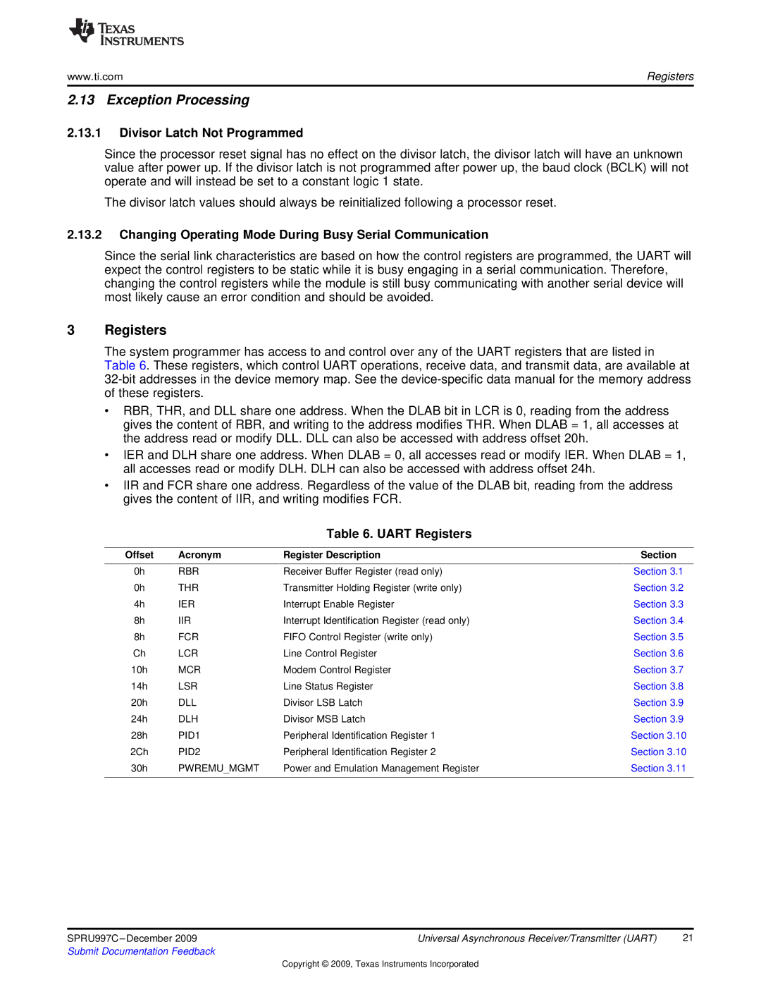
Table 6. UART Registers
Offset | Acronym | Register Description | Section |
0h | RBR | Receiver Buffer Register (read only) | Section 3.1 |
0h | THR | Transmitter Holding Register (write only) | Section 3.2 |
4h | IER | Interrupt Enable Register | Section 3.3 |
8h | IIR | Interrupt Identification Register (read only) | Section 3.4 |
8h | FCR | FIFO Control Register (write only) | Section 3.5 |
Ch | LCR | Line Control Register | Section 3.6 |
10h | MCR | Modem Control Register | Section 3.7 |
14h | LSR | Line Status Register | Section 3.8 |
20h | DLL | Divisor LSB Latch | Section 3.9 |
24h | DLH | Divisor MSB Latch | Section 3.9 |
28h | PID1 | Peripheral Identification Register 1 | Section 3.10 |
2Ch | PID2 | Peripheral Identification Register 2 | Section 3.10 |
30h | PWREMU_MGMT | Power and Emulation Management Register | Section 3.11 |
|
|
|
|
SPRU997C | Universal Asynchronous Receiver/Transmitter (UART) | 21 |
Submit Documentation Feedback |
|
|
Copyright © 2009, Texas Instruments Incorporated