Architecture | www.ti.com |
2.3Signal Descriptions
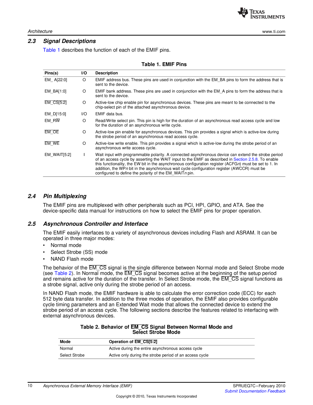
Table 1 describes the function of each of the EMIF pins.
|
|
|
|
|
|
|
| Table 1. EMIF Pins |
|
|
|
| |||||
| Pins(s) | I/O | Description | |||||
|
|
|
| |||||
| EM_ A[22:0] | O | EMIF address bus. These pins are used in conjunction with the EM_BA pins to form the address that is | |||||
|
|
|
|
|
|
|
| sent to the device. |
| EM_BA[1:0] | O | EMIF bank address. These pins are used in conjunction with the EM_A pins to form the address that is | |||||
|
|
|
|
|
|
|
| sent to the device. |
|
|
| O | |||||
| EM_CS[5:2] | |||||||
|
|
|
|
|
|
|
| |
| EM_D[15:0] | I/O | EMIF data bus. | |||||
|
|
|
|
| O | Read/Write select pin. This pin is high for the duration of an asynchronous read access cycle and low | ||
| EM_RW | |||||||
|
|
|
|
|
|
|
| for the duration of an asynchronous write cycle. |
|
|
|
|
|
| O | ||
| EM_OE | |||||||
|
|
|
|
|
|
|
| the strobe period of an asynchronous read access cycle. |
|
|
|
|
|
|
| O | |
| EM_WE | |||||||
|
|
|
|
|
|
|
| asynchronous write access cycle. |
| EM_WAIT[5:2] | I | Wait input with programmable polarity. A connected asynchronous device can extend the strobe period | |||||
|
|
|
|
|
|
|
| of an access cycle by asserting the WAIT input to the EMIF as described in Section 2.5.8. To enable |
|
|
|
|
|
|
|
| this functionality, the EW bit in the asynchronous configuration register (ACFGn) must be set to 1. In |
|
|
|
|
|
|
|
| addition, the WPn bit in the asynchronous wait cycle configuration register (AWCCR) must be |
|
|
|
|
|
|
|
| configured to define the polarity of the EM_WAITn pin. |
|
|
|
|
|
|
|
|
|
2.4Pin Multiplexing
The EMIF pins are multiplexed with other peripherals such as PCI, HPI, GPIO, and ATA. See the
2.5Asynchronous Controller and Interface
The EMIF easily interfaces to a variety of asynchronous devices including Flash and ASRAM. It can be operated in three major modes:
•Normal mode
•Select Strobe (SS) mode
•NAND Flash mode
The behavior of the EM_CS signal is the single difference between Normal mode and Select Strobe mode (see Table 2). In Normal mode, the EM_CS signal becomes active at the beginning of the setup period and remains active for the duration of the transfer. In Select Strobe mode, the EM_CS signal functions as a strobe signal, active only during the strobe period of an access.
In NAND Flash mode, the EMIF hardware is able to calculate the error correction code (ECC) for each 512 byte data transfer. In addition to the three modes of operation, the EMIF also provides configurable cycle timing parameters and an Extended Wait mode that allows the connected device to extend the strobe period of an access cycle. The following sections describe the features related to interfacing with external asynchronous devices.
Table 2. Behavior of EM_CS Signal Between Normal Mode and
Select Strobe Mode
|
|
|
|
Mode | Operation of EM_CS[5:2] | ||
Normal | Active during the entire asynchronous access cycle | ||
Select Strobe | Active only during the strobe period of an access cycle | ||
|
|
|
|
10 | Asynchronous External Memory Interface (EMIF) | SPRUEQ7C |
|
| Submit Documentation Feedback |
Copyright © 2010, Texas Instruments Incorporated
