www.ti.com | Use Cases |
3.2.3Example Using Hynix HY27UA081G1M
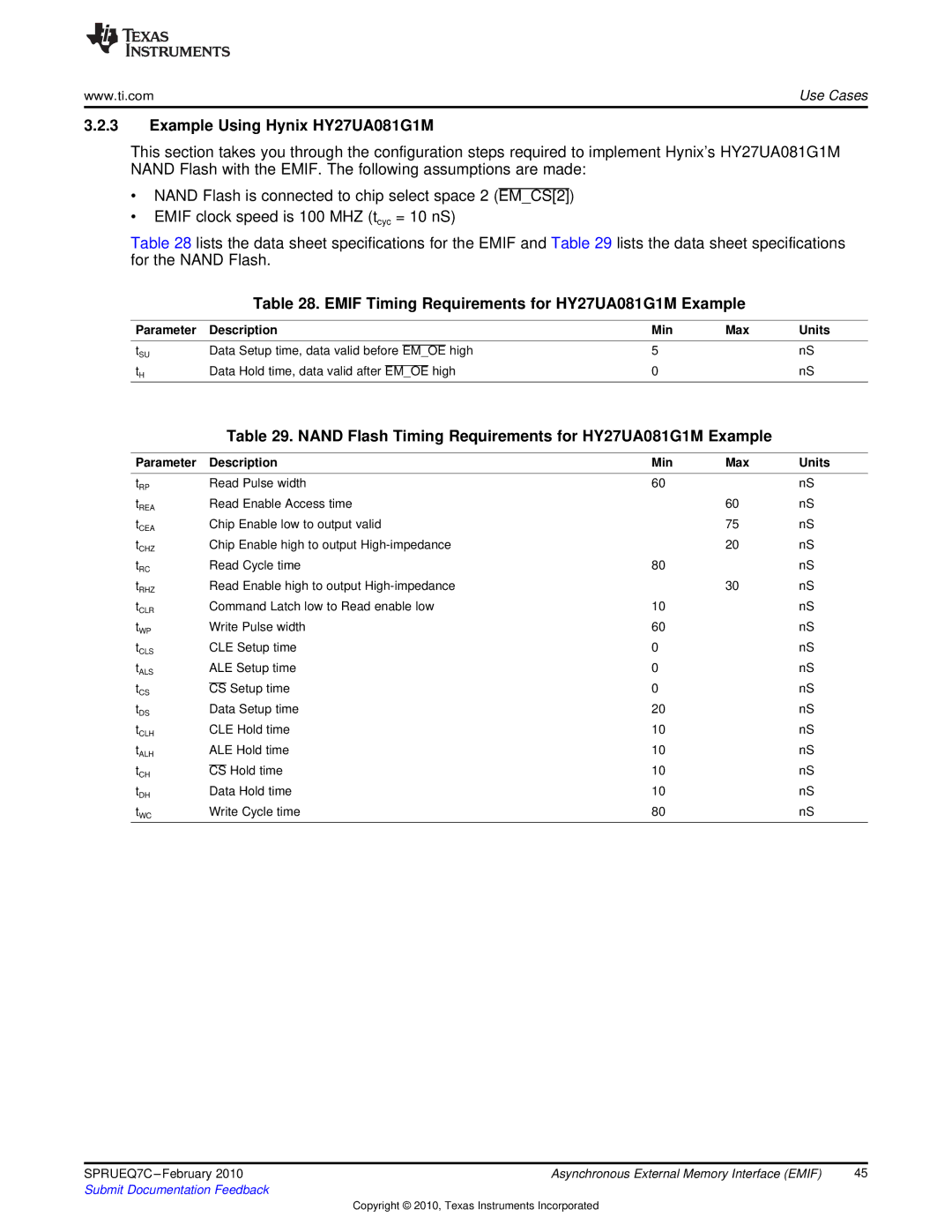
This section takes you through the configuration steps required to implement Hynix’s HY27UA081G1M NAND Flash with the EMIF. The following assumptions are made:
•NAND Flash is connected to chip select space 2 (EM_CS[2])
•EMIF clock speed is 100 MHZ (tcyc = 10 nS)
Table 28 lists the data sheet specifications for the EMIF and Table 29 lists the data sheet specifications for the NAND Flash.
Table 28. EMIF Timing Requirements for HY27UA081G1M Example
Parameter | Description | Min | Max | Units | ||||
tSU | Data Setup time, data valid before |
|
| high | 5 |
| nS | |
EM_OE |
| |||||||
tH | Data Hold time, data valid after |
|
| high | 0 |
| nS | |
EM_OE |
| |||||||
Table 29. NAND Flash Timing Requirements for HY27UA081G1M Example
Parameter | Description | Min | Max | Units | |
tRP | Read Pulse width | 60 |
| nS | |
tREA | Read Enable Access time |
| 60 | nS | |
tCEA | Chip Enable low to output valid |
| 75 | nS | |
tCHZ | Chip Enable high to output |
| 20 | nS | |
tRC | Read Cycle time | 80 |
| nS | |
tRHZ | Read Enable high to output |
| 30 | nS | |
tCLR | Command Latch low to Read enable low | 10 |
| nS | |
tWP | Write Pulse width | 60 |
| nS | |
tCLS | CLE Setup time | 0 |
| nS | |
tALS | ALE Setup time | 0 |
| nS | |
tCS |
| Setup time | 0 |
| nS |
CS |
| ||||
tDS | Data Setup time | 20 |
| nS | |
tCLH | CLE Hold time | 10 |
| nS | |
tALH | ALE Hold time | 10 |
| nS | |
tCH |
| Hold time | 10 |
| nS |
CS |
| ||||
tDH | Data Hold time | 10 |
| nS | |
tWC | Write Cycle time | 80 |
| nS | |
SPRUEQ7C | Asynchronous External Memory Interface (EMIF) | 45 |
Submit Documentation Feedback |
|
|
Copyright © 2010, Texas Instruments Incorporated