R
Chapter 1: Introduction
•
•
•256 input and 256 output ports for easy expansion and enhancement
•Automatic
•Predictable performance, always two clock cycles per instruction, up to 200 MHz or 100 MIPS in a
•Fast interrupt response;
•Optimized for Xilinx
•Assembler,
| 1Kx18 | ProgramCounter | (PC) | 31x10 | CALL/RETURN | Stack |
|
| PORT_ID | |||
Instruction | Scratchpad RAM |
|
|
| ||||||||
| PROM |
|
|
| ||||||||
|
|
|
|
|
|
| ||||||
|
|
|
|
|
| OUT_PORT | ||||||
|
|
|
|
|
|
|
| |||||
Instruction |
|
|
|
|
|
|
|
|
| Flags |
| |
|
|
|
|
|
| Constants |
| Z | Zero | |||
| Decoder |
|
|
|
|
|
|
|
|
| ||
|
|
|
|
|
|
|
|
|
| C | Carry | |
|
|
|
|
|
|
|
|
|
|
| ||
INTERRUPT |
|
|
|
| 16 |
|
|
| ||||
| Enable |
|
|
|
| Operand 1 | ALU |
| ||||
IE |
|
|
|
| s0 | s1 | s2 | s3 |
| |||
|
|
|
|
|
| |||||||
|
|
|
|
|
| s4 | s5 | s6 | s7 |
|
|
|
IN_PORT |
|
|
|
| s8 | s9 | sA | sB |
|
|
| |
|
|
|
|
|
| sC | sD | sE | sF |
|
|
|
|
|
|
|
|
|
|
|
|
| Operand 2 |
|
|
|
|
|
|
|
|
|
|
|
|
|
| UG129_c1_01_051204 |
|
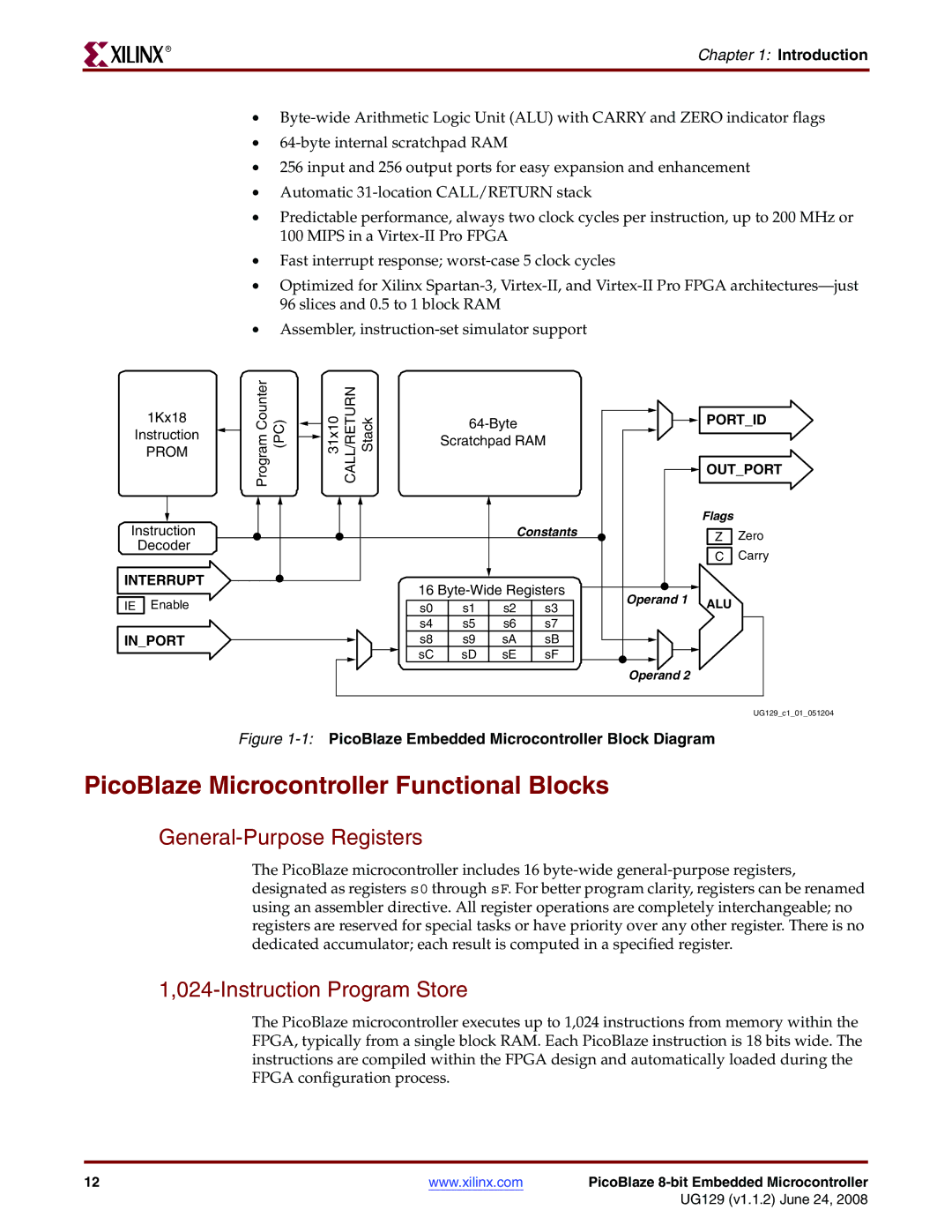
| Figure |
| |||||||||
PicoBlaze Microcontroller Functional Blocks
General-Purpose Registers
The PicoBlaze microcontroller includes 16
1,024-Instruction Program Store
The PicoBlaze microcontroller executes up to 1,024 instructions from memory within the FPGA, typically from a single block RAM. Each PicoBlaze instruction is 18 bits wide. The instructions are compiled within the FPGA design and automatically loaded during the FPGA configuration process.
12 | www.xilinx.com | PicoBlaze |
UG129 (v1.1.2) June 24, 2008