UG129 v1.1.2 June 24
PicoBlaze 8-bit Embedded Microcontroller User Guide
Version Revision
Revision History
Limitations
Limited Warranty and Disclaimer
Limitation of Liability
Technical Support Limitations
Preface Acknowledgments
Acknowledgments
About This Guide
Guide Contents
Preface About This Guide
Table of Contents
Interrupts
Performance
Appendix C PicoBlaze Instruction Set and Event Reference
Introduction
PicoBlaze Microcontroller Features
General-Purpose Registers
PicoBlaze Microcontroller Functional Blocks
Instruction Program Store
Introduction
Flags
Arithmetic Logic Unit ALU
Byte Scratchpad RAM
Input/Output
Program Counter PC
Reset
Program Flow Control
CALL/RETURN Stack
Why the PicoBlaze Microcontroller?
Why the PicoBlaze Microcontroller?
Why Use a Microcontroller within an FPGA?
Weaknesses
Strengths
Signal Direction Description
PicoBlaze Interface Signals
PicoBlaze Interface Signal Descriptions
Readstrobe
1PicoBlaze Instruction Set alphabetical listing
PicoBlaze Instruction Set
Enable Interrupt
Returni Disable
Address Spaces
Instruction 1Kx18 Direct
PicoBlaze Instruction Set
Processing Data
Logic Instructions
3Inverting an Individual Bit Location
2Complementing a Register Value
Arithmetic Instructions
616-Setting a Bit Location
SUB and Subcy Subtract Instructions
10Incrementing and Decrementing a Register
Multiplication
148-bit by 8-bit Multiply Routine Produces a 16-bit Product
Division
168-bit by 8-bit Multiply Routine Using Hardware Multiplier
18Loading a Register with Itself Acts as a NOP Instruction
No Operation NOP
Test and Compare
Setting and Clearing Carry Flag
22The Test Instruction Affects the Zero Flag
Shift and Rotate Instructions
25Generate Parity for a Register Using the Test Instruction
5PicoBlaze Rotate Instructions Rotate Left Rotate Right
SRX
Program Flow Control
Moving Data
6Instruction Conditional Execution Description
Program Flow Control
CALL/RETURN
Program Flow Control
UG129 v1.1.2 June 24
1Simple Interrupt Logic
Interrupts
2Example Interrupt Flow
Example Interrupt Flow
Example Interrupt Flow
3Interrupt Timing Diagram
Interrupts
Address Modes
Scratchpad RAM
Direct Addressing
Indirect Addressing
Scratchpad RAM
Implementing a Look-Up Table
Stack Operations
Stack Operations
Fifo Operations
Scratchpad RAM
Portid Port
Input and Output Ports
1INPUT Operation and Fpga Interface Logic
Input Operations
PORTID70
Input Operations
INPORT70
Register s0
Input and Output Ports
Applications with Few Input Sources
Readstrobe Interaction with FIFOs
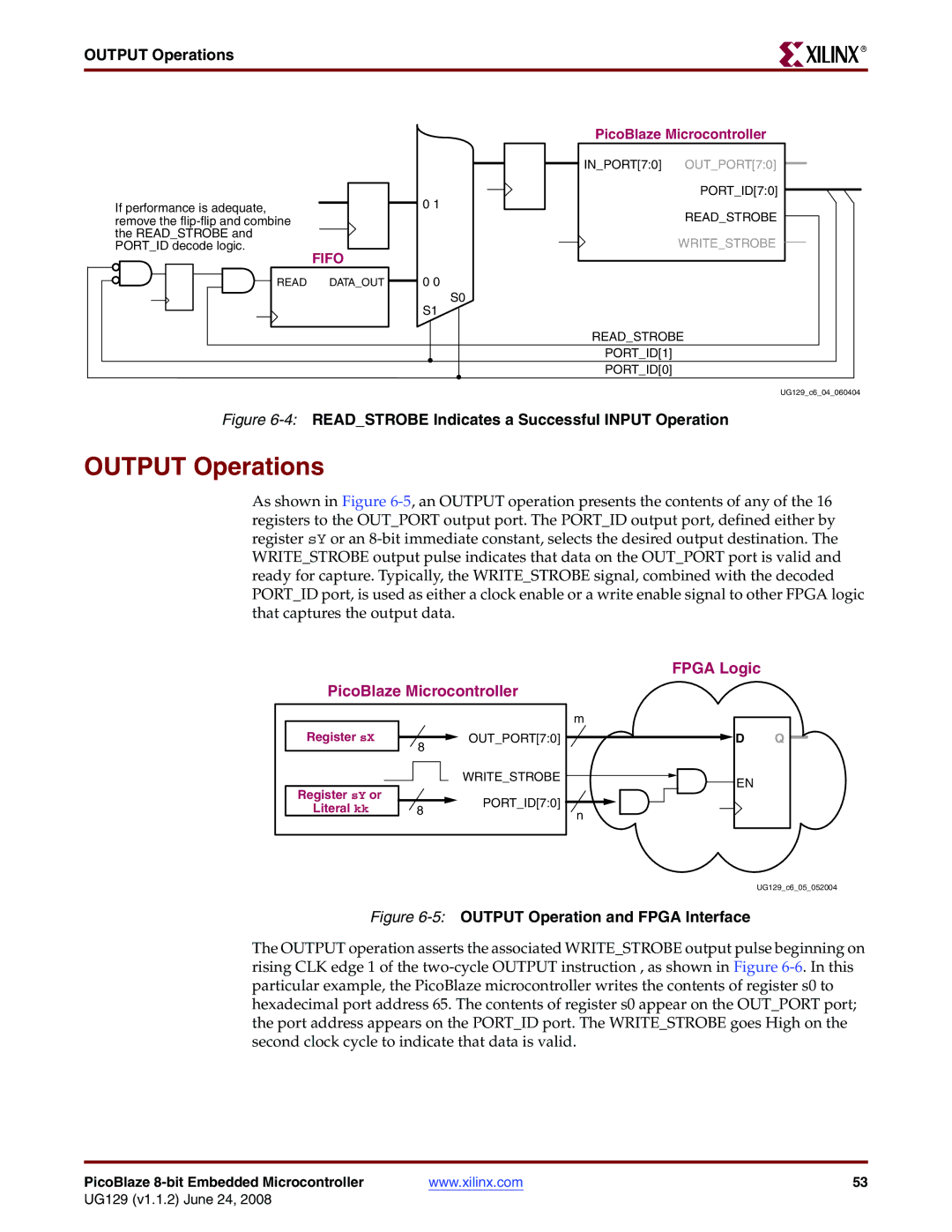
Output Operations
Output Operations
Fpga Register
Simple Output Structure for Few Output Destinations
8Use Constant Directives to Declare Output Port Addresses
9Pipelining the Portid Decoding Improves Performance
Pipelining for Maximum Performance
Pipelining for Maximum Performance
Effective Pipelining Improves Read Performance
Repartitioning the Design for Maximum Performance
Standard Configuration Single 1Kx18 Block RAM
Instruction Storage Configurations
Two PicoBlaze Microcontrollers Share a 1Kx18 Code Image
Instruction Storage Configurations
Distributed ROM Instead of Block RAM
6Using Distributed ROM for Instruction Memory
Instruction Storage Configurations
Input Clock Frequency
Performance
Predicting Executing Performance
Frequency
Performance
Assembler
PicoBlaze Development Tools
PicoBlaze Development Tools
Assembly Errors
Input and Output Files
Mediatronix pBlazIDE
Configuring pBlazIDE for the PicoBlaze Microcontroller
4Example of How Kcpsm Source Code Converts to pBlazIDE Code
Importing KCPSM3 Code into pBlazIDE
Directives
Differences Between the KCPSM3 Assembler and pBlazIDE
Differences Between the KCPSM3 Assembler and pBlazIDE
Function KCPSM3 Directive PBlazIDE Directive
PicoBlaze Development Tools
KCPSM3 Module
Using the PicoBlaze Microcontroller in an Fpga Design
Vhdl Design Flow
Using the PicoBlaze Microcontroller in an Fpga Design
Connecting the Program ROM
Generating the Program ROM using progrom.coe
Black Box Instantiation of KCPSM3 using KCPSM3.ngc
Generating an ESC Schematic Symbol
Black Box Instantiation of KCPSM3 using KCPSM3.ngc
Using the PicoBlaze Microcontroller in an Fpga Design
Naming or Aliasing Registers
Assembler Directives
Locating Code at a Specific Address
Naming the Program ROM Output File
Defining Constants
Defining I/O Ports pBlazIDE
PBlazIDE
Defining I/O Ports pBlazIDE
Input Ports
Output Ports
5Example of pBlazIDE Dsout Directive
Input/Output Ports
Custom Instruction Op-Codes
Custom Instruction Op-Codes
Assembler Directives
Simulating PicoBlaze Code
Instruction Set Simulation with pBlazIDE
Instruction Set Simulation with pBlazIDE
Simulator Control Buttons
2pBlazIDE Simulator Control Buttons Function Assemble
Edit
Step Over
Run
Run to Cursor
Pause
Turbocharging Simulation using FPGAs
Turbocharging Simulation using FPGAs
Simulating PicoBlaze Code
Related Materials and References
Chapter Related Materials and References
KCPSM3 Syntax
Example Program Templates
Appendix Example Program Templates
PBlazIDE Syntax
ADD sX, Operand -Add Operand to Register sX
PicoBlaze Instruction Set and Event Reference
Appendix PicoBlaze Instruction Set and Event Reference
Addcy sX, Operand -Add Operand to Register sX with Carry
SX, Operand Logical Bitwise and Register sX with Operand
SX, Operand Logical Bitwise and Register sX with Operand
Examples
Table C-1CALL Instruction Conditions Description
Condition
Figure C-4COMPARE Operation
Compare sX, Operand Compare Operand with Register sX
Disable Interrupt Disable External Interrupt Input
Disable Interrupt Disable External Interrupt Input
Enable Interrupt Enable External Interrupt Input
KCPSM3 Instruction PBlazIDE Instruction
Figure C-5FETCH Operation
Portid Å Operand SX Å Inport PC Å PC +
Interrupt Event, When Enabled
Table C-2JUMP Instruction Conditions Description
Load sX, Operand Load Register sX with Operand
Or sX, Operand Logical Bitwise or Register sX with Operand
Or sX, Operand Logical Bitwise or Register sX with Operand
Figure C-7OUTPUT Operation and Fpga Interface Logic
Table C-3PicoBlaze Reset Values Resource Reset Event Effect
Reset Event
Reset Event
Table C-4RETURN Instruction Conditions Description
PBlazIDE Equivalent RET, RET C, RET NC, RET Z, RET NZ
RR sX Rotate Right Register sX
RL sX Rotate Left Register sX
Table C-5Rotate Left RL Operation
Table C-6Rotate Right RR Operation
Table C-7Shift Left Operations
SL 0 1 X a sX Shift Left Register sX
SL 0 1 X a sX Shift Left Register sX
SR 0 1 X a sX Shift Right Register sX
Shift Right with ‘ 0’ fill
Figure C-8STORE Operation
Store sX, sY
SUB sX, Operand -Subtract Operand from Register sX
Figure C-10SUBCY Instruction
Registers sX Flags CARRY, Zero PBlazIDE Equivalent Subc
Figure C-11ZERO Flag Logic for Test Instruction
PicoBlaze 8-bit Embedded Microcontroller 117
XOR sX, Operand Logical Bitwise XOR Register sX with Operand
Table D-1PicoBlaze Instruction Codes
Instruction Codes
Jump Z
PicoBlaze 8-bit Embedded Microcontroller 121
Appendix Instruction Codes
Reg Description
Register and Scratchpad RAM Planning Worksheets
Registers
Loc Description
Scratchpad RAM
Appendix Register and Scratchpad RAM Planning Worksheets