Chapter 8 Details of Usage
Page 8 - 6 |
| Byte and Word Swapping |
Note
Offset + x values are in opposite order for Intel Processors
RF3880
Swapping
Options
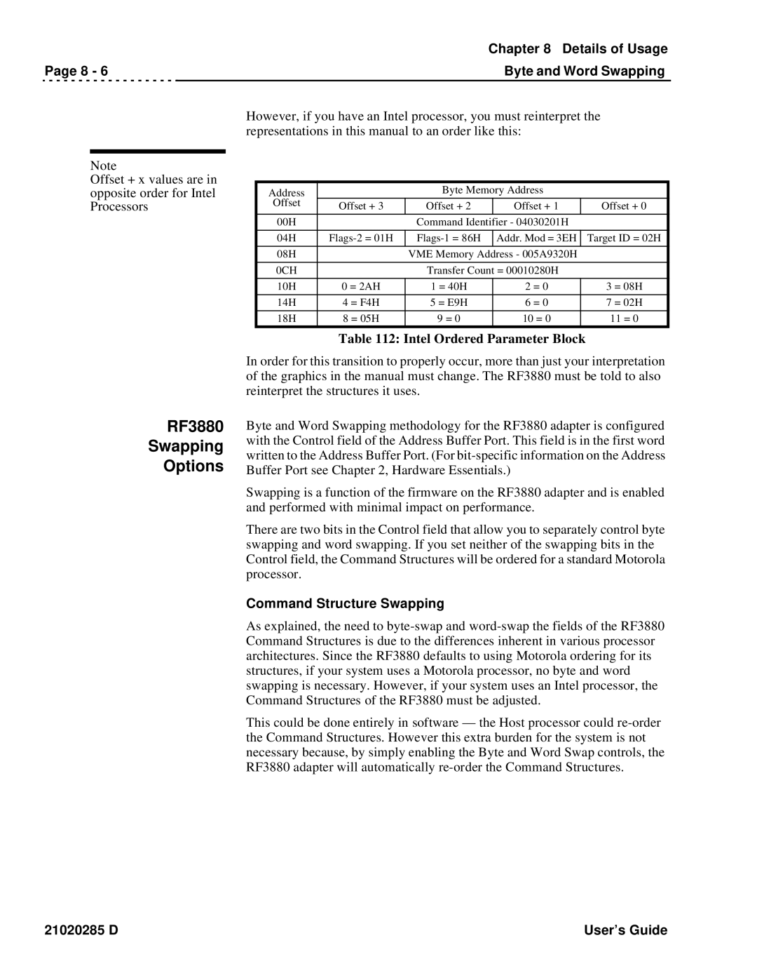
However, if you have an Intel processor, you must reinterpret the representations in this manual to an order like this:
Address |
| Byte Memory Address |
| |
Offset | Offset + 3 | Offset + 2 | Offset + 1 | Offset + 0 |
| ||||
|
|
|
|
|
00H |
| Command Identifier - 04030201H |
| |
|
|
|
|
|
04H | Addr. Mod = 3EH | Target ID = 02H | ||
|
|
|
|
|
08H |
| VME Memory Address - 005A9320H |
| |
|
|
|
| |
0CH |
| Transfer Count = 00010280H |
| |
10H | 0 = 2AH | 1 = 40H | 2 = 0 | 3 = 08H |
|
|
|
|
|
14H | 4 = F4H | 5 = E9H | 6 = 0 | 7 = 02H |
|
|
|
|
|
18H | 8 = 05H | 9 = 0 | 10 = 0 | 11 = 0 |
|
|
|
|
|
Table 112: Intel Ordered Parameter Block
In order for this transition to properly occur, more than just your interpretation of the graphics in the manual must change. The RF3880 must be told to also reinterpret the structures it uses.
Byte and Word Swapping methodology for the RF3880 adapter is configured with the Control field of the Address Buffer Port. This field is in the first word written to the Address Buffer Port. (For
Swapping is a function of the firmware on the RF3880 adapter and is enabled and performed with minimal impact on performance.
There are two bits in the Control field that allow you to separately control byte swapping and word swapping. If you set neither of the swapping bits in the Control field, the Command Structures will be ordered for a standard Motorola processor.
Command Structure Swapping
As explained, the need to
This could be done entirely in software — the Host processor could
21020285 D | User’s Guide |