IBM eServer zSeries 990 Technical Guide
Page
IBM eServer zSeries 990 Technical Guide
Second Edition April
This document created or updated on April 7
Iii
Iv IBM eServer zSeries 990 Technical Guide
Contents
6947TOC.fm
6947TOC.fm
Appendix B. Fiber optic cabling services
6947spec.fm
Eckd
Trademarks
First Edition authors
Team that wrote this redbook
Comments welcome
Become a published author
IBM zSeries 990 overview
Balanced system design
Escon
Introduction
Model upgrade paths
Z990 models
General rules
Concurrent Processor Unit PU conversions
System functions and features
Processor
Model downgrades
Memory
Self-Timed Interconnect STI
Channel Subsystem CSS
Spanned channels
Physical Channel IDs PCHIDs and Chpid Mapping Tool
Cage
7 I/O connectivity
Up to 120 Ficon Express channels
Up to 1024 Escon channels
Ficon Cascaded Directors
Ficon CTC function
1000BASE-T Ethernet
Checksum Offload for Linux and z/OS when Qdio mode
OSA-Express
Gigabit Ethernet
OSA-Express ATM
Cryptographic CP Assist for cryptographic function
Parallel channels and converters
Token Ring
PCI Cryptographic Accelerator feature Pcica
PCI X-Cryptographic Coprocessor Pcixcc feature
Parallel Sysplex support
Internal Coupling IC
ICB-2 Integrated Cluster Bus
ICB-3 Integrated Cluster Bus
ICB-4 Integrated Cluster Bus
Hardware consoles
Intelligent Resource Director IRD
On/Off Capacity Upgrade on Demand On/Off CoD
Concurrent upgrades
Capacity Upgrade on Demand CUoD
Customer Initiated Upgrade CIU
32 CPS
Performance
Software
Reliability, Availability, Serviceability RAS
Unix System Services
Traditional database/transaction workloads
ZSeries File System zFS
OS/390 & z/OS
Software support
Compatibility and exploitation
Linux on zSeries and Linux for S/390
Software pricing
Linux
VSE
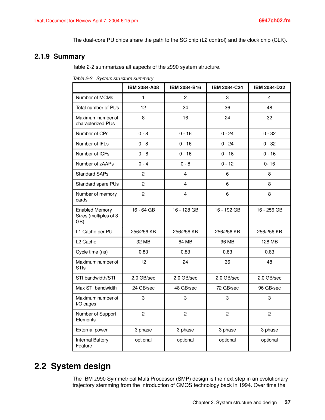
Summary
System structure and design
Book concept
System structure
Cooling
Power
Hybrid cooling system
Models
Memory Sizes
New build 2084 physical memory card distribution
Memory sparing
Memory upgrades
Book replacement and memory
Ring Topology
MCM
MCM
Connectivity
STI connectors Book front view
Book upgrade
Frames and cages
Book replacement and connectivity
Frame
Cages
Capacitors
MCM
PU, SC, and SD chips
SC chip
SD chip
IBM 2084-A08 IBM 2084-B16 IBM 2084-C24 IBM 2084-D32
System design
Design highlights
Book design
12 Logical book structure
Processor Unit design
Dual External Time Reference
Superscalar processor
Asymmetric mirroring for error detection
CP Assist for Cryptographic Function
Compression Unit on a chip
Without BHT With BHT
Processor Branch History Table BHT
Instruction grouping
Ieee Floating Point
Translation Lookaside Buffer
Instruction fetching and instruction decode
Processor unit functions
Integrated Facilities for Linux
Central Processors
Internal Coupling Facilities
Dynamic ICF Expansion
Dynamic Coupling Facility Dispatching
ZSeries Application Assist Processors
ZAAPs and Lpar definitions
Purpose of a zAAP
System Assist Processors
Software support
Optional additional orderable SAPs
Reserved processors
Processor unit characterization
Optionally assignable SAPs
Sparing rules
Transparent CP, IFL, ICF, zAAP, and SAP sparing
Application preservation
Dynamic SAP sparing and reassignment
Dynamic Memory sparing
Memory design
Partial Memory Restart
Memory allocation
Central storage CS
Expanded storage ES
Lpar single storage pool
Hardware System Area HSA
Modes of operation
VSE/ESA
Logical Partitioning overview
Processors
Channels
Memory
Logically Partitioned Mode
Dynamic Add/Delete of a logical partition name
Model configurations
ZAAP
Upgrades
Unassigned CP
Unassigned IFL
Z990 Models 2084-A08 2084-B16 2084-C24 2084-D32
Software models
Z990 Models Software
PU conversions
From
Software model MSU values
Software MSU/ Pricing Model
Hardware Management Console and Support Elements
Storage operations
ESA/390 mode
Operating
Definition Definable
Architecture mode
ESA/390 TPF mode
Coupling Facility mode
Linux Only mode
Lpar storage granularity
Reserved storage
12 I/O subsystem
Lpar Dynamic Storage Reconfiguration DSR
Cage Front Pchid ## Rear Pchid ##
Channel Subsystem
Logical Channel Subsystem Lcss
Physical Channel ID Pchid
O system structure
Overview
CEC Cage 1st I/O Cage standard
I/O cages
Domain Slots in domain
Board
Z990 Model Number of books Number of MBAs Number of STIs
STIs and I/O cage connections
Cage
ESTI-M card
Balancing I/O connections
STI-2 Extender card
STI-3 Extender card
STI Links Cards
STI links balancing across books and MBAs
2084-B16 CEC Cage
Book
2084-D32 CEC Cage
STI Rebalance feature Feature Code
Cage
Upgrade example with the STI Rebalance feature FC
STIs
Port balancing across MBAs and books
Card types Feature Codes FC
I/O and cryptographic feature cards
1 I/O feature cards
Feature cards no longer supported
Cryptographic feature cards
Cryptographic feature card no longer supported
Cryptographic card types Feature Codes FC
PCHIDs 121 131 Slots
Physical Channel IDs PCHIDs
Pchid Report example
CEC cage book Pchid numbers
Z990 Chipd Mapping Tool CMT
Connectivity
6947ch03.fm
Spanned and Shared channels
Feature code Feature name Connector type Cable type
Features cables and connectors
Escon channel
Z990 16-port Escon feature
Escon channel port enablement feature
Port Escon channel sparing
Fiber Quick Connect FQC for Escon Quick Connect
Ficon Express features
Ficon Express LX feature
Ficon channel
Ficon channel in Fibre Channel Protocol FCP mode
Ficon Express SX feature
Z990 adapter interruptions enhancement for FCP
Z990 FCP Scsi IPL feature enabler FC
OSA-Express adapter
Z990 FCP concurrent patch
OSA-Express GbE LX feature code
OSA-Express GbE SX feature code
OSA-Express GbE LX feature code 2364, upgrade only
OSA-Express 1000BASE-T Ethernet feature code
OSA-Express GbE SX feature code 2365, upgrade only
OSA-Express Integrated Console Controller OSA-ICC
OSA-Express Fast Ethernet feature code 2366, upgrade only
OSA-Express Token Ring feature code
Checksum offload for IPv4 packets when in Qdio mode
HiperSockets function
Z990 coupling link features
Coupling Facility links
Z990 adapter interruptions enhancement for Qdio
RPQ 8P2197 Extended distance option
ISC-3 link
Mode
ICB-4 link
ICB-3 link
ICB-2 link
External Time Reference ETR feature
IC links
Z990 ICB links summary
Cryptographic features
Pcix Cryptographic Coprocessor Pcixcc feature
PCI Cryptographic Accelerator Pcica feature
6947ch03.fm
109
Channel Subsystem
Logical Channel Subsystem structure
Multiple Logical Channel Subsystem Lcss
Logical partition number
Multiple Image Facility MIF
Logical Partition ID
Logical partition identifier
MIF Image ID Mifid
Logical partition name
Dynamic Addition or Deletion of a logical partition name
Physical Channel ID Pchid
Z990 Lcss connectivity
Channel spanning
Lcss configuration management
IBM Configurator for e-business e-Config
Hardware Configuration Dialog HCD
IBM z990 Chpid Mapping Tool CMT
1 z990 configuration management
Z990
LCSS-related numbers
6947ch04.fm
119
Cryptography
Cryptographic function support
Cryptographic Synchronous functions
Cryptographic Asynchronous functions
Cryptography
CP Assist for Cryptographic Function Cpacf
Z990 Cryptographic processors
Pcix Cryptographic Coprocessor Pcixcc
PCI Cryptographic Accelerator Pcica feature
Cryptographic hardware features
Pcix Cryptographic Coprocessor feature
Crypto
Configuration rules
Pcica feature
4 z990 cryptographic feature codes
Cryptographic features comparison
TKE workstation feature
Functions or Attributes
Private keys Public Key Encrypt PKE support for MRP function
Software requirements
6947ch05.fm
Operating system
6947ch05.fm
133
Software support
Operating system support
Z/OS software support
Compatibility support for z/OS
Compatibility support requirements
Z990 Compatibility for selected OS/390, and z/OS releases
Z990
Compatibility support restrictions
OS V1.5 Support
OS V1.4 z990 Compatibility Support feature
OS V1.4 z990 Exploitation Support feature
Exploitation support for z/OS
Dynamic addition and deletion of a logical partition name
Processors within a single logical partition
ZSeries Application Assist Processor zAAP
JVM
HCD support
Automation changes
SMF support
Ickdsf requirements
RMF support
Automation
Icsf support
Additional exploitation support considerations
Standalone dump
D M=CPU command output
Extended Channel Measurement Block
Switch ID =
Greater than 15 logical partitions
Z/VM software support
Dynamic activates for hardware changes
Dynamic Chpid management
Z/VSE and VSE/ESA software support
TPF software support
Linux software support
V1.4
Summary of software requirements
Summary of z/OS and OS/390 software requirements
Software Requirements OS/390 V1.6 a
V4.1
Software Requirements
Linuxon
V5.1 V4.4 V3.1
OSA-ICC
Workload License Charges
Concurrent upgrades considerations
Processor Identification
Version CPU identification number Machine Code Type number
Channel to Channel links
153
Sysplex functions
Sysplex LPARs
Parallel Sysplex
Parallel Sysplex described
Sysplex LPARs CF02
Systems management
Continuous application availability
High capacity
Dynamic workload balancing
Single system image
Resource sharing
Message Time Ordering
Sysplex configurations and Sysplex Timer considerations
Sysplex and Coupling Facility considerations
Parallel Sysplex summary
6947ch07.fm
Example 7-1 Display ETR
Cfcc enhanced patch apply
Coupling Facility and Cfcc considerations
Minimum software levels a
Cflevel
Link Type Z990 Max
Coupling Facility link connectivity
Link Type Z990 Max Maximum number of links per z990
Peer mode links
Meaning of Partition
ICF processor assignments
Function Setup
Z990 Dynamic CF Dispatching shared CPs or shared ICF PUs
Dynamic CF dispatching and dynamic ICF expansion
Benefits
System-managed CF structure duplexing
CF Structure Duplexing
Configuration planning
Z800/z900/z990/z890/G5/G6z800/z900/z990/z890/G5/G6
GDPS/PPRC
Geographically Dispersed Parallel Sysplex
ZSeries
GDPS/PPRC HyperSwap
Unplanned HyperSwap
Planned HyperSwap
Business Continuity for Linux guests
GDPS/PPRC Management for Open Systems LUNs
GDPS/PPRC over Fiber Channel links
Gdps FlashCopy V2 support
GDPS/XRC
Application
Gdps and Capacity Backup CBU
Recovery
Site
IRD overview
Intelligent Resource Director
Lpar CPU management
Value of CPU management
Dynamic Channel Path Management
Value of Dynamic Channel Path Management
Channel Subsystem Priority Queueing
WLM and Channel Subsystem priority
Value of Channel Subsystem Priority Queueing
Workload type Priority
Disabling Dynamic Channel Path Management
Automatic I/O interface reset
Special considerations and restrictions
Unique Lpar cluster names
System automation I/O operations
References
6947ch07.fm
185
Capacity upgrades
Concurrent PU conversions
Concurrent upgrades
Licensed Internal Code LIC-based upgrades
Concurrent hardware installation upgrades
Planned upgrades
Model upgrades
Function Upgrades Via Type Process
Capacity Upgrade on Demand CUoD
Unplanned upgrades
Capacity upgrade functions
6947ch08.fm
CUoD + 1 CP + 2 IFLs
CUoD for processors
CUoD for memory
CUoD + 16 GB + Model upgrade
+ 8 Escon
CUoD for I/O
Plan Ahead concurrent conditioning
Customer Initiated Upgrade CIU
CIU Registration and Agreed Contract for CIU
Internet
Ordering
Order and fulfillment process
CIU order example
Z990 Model Conversion screen
Activation
On/Off Capacity on Demand On/Off CoD
CIU upgrade selection screen
6947ch08.fm
Initiation
Termination
Activation/Deactivation
Repair capability during On/Off CoD
Capacity BackUp CBU
Upgrade Capability during On/Off CoD
Software
6947ch08.fm
Image upgrades
Activation/deactivation of CBU
CBU activation
CBU deactivation
Capacity BackUp operation example
Automatic CBU enablement for Gdps
CBU testing
Processors
Nondisruptive upgrades
Upgrade scenarios
Memory
PCI Cryptographic coprocessors
LP1 LP2
Shared logical partitions upgrade
LP1 LP2 LP3
Dedicated and shared logical partitions upgrade
Shared partitions and zAAP upgrade
LP1 LP2
Dedicated, shared partitions and IFL upgrade
LP2
Dedicated, shared partitions and ICF upgrade
Reasons for disruptive upgrades
Planning for nondisruptive upgrades
Recommendations to avoid disruptive upgrades
Capacity planning considerations
Considerations when installing additional books
Additional performance improvements for e-business
Balanced system design
16 shows a two-book z990 server logical view
Multi-book structure
Superscalar processors
Book
Secure encrypted transactions with higher performance
Integrated hardware and system assists
ZSeries Application Assist Processors zAAPs
Cryptographic function on every Processor Unit PU
Performance assists for Linux and z/VM
Capacity measurements
Internal Throughput Rate ITR and ITR Ratio Itrr
Large Systems Performance Reference Lspr
Lspr workloads prior to z990
Lspr workloads for z990
Operating system Workload type Workload description
Lspr workloads for z990 Lpar Mode
6947ch08.fm
OLTP-T
New predefined z/OS workload mixes
Z990 Lspr tables
229
Environmentals
Power and cooling requirements
Power consumption
Internal Battery Feature
Cooling requirements
Weights
Emergency power-off
Configuration
Frames Width mm Depth mm Height mm
Dimensions
233
Appendix A. Hardware Management Console HMC
LAN
LAN
Z990 Hardware Management Console
Token-Ring LAN
Token ring only wiring scenario
Additional token ring only wiring scenario
Ethernet only one-path wiring scenario
Additional connections to the Ethernet LAN
Figure A-5 Ethernet only one path wiring scenario
Ethernet only two-path wiring scenario
Figure A-7 Ethernet only two-path wiring scenario
Token ring and Ethernet wiring scenario
Additional connections to the Token Ring LAN
Remote operations
Support Element
Z990 HMC enhancements
Z990 HMC Integrated 3270 Console
Increased Console tasks performed log
Optional strict password rules supported
Z990 HMC Integrated Ascii Console support
Enhanced logging facilities
SNA Operations Management for Operations Automation
6947axA.fm
247
Appendix B. Fiber optic cabling services
Fiber optic cabling services from IBM
249
Summary
6947axB.fm
IBM Redbooks
Other publications
251
Online resources
How to get IBM Redbooks
253
Glossary
EMIF. See Escon Multiple Image Facility
Fiber optic cable. See optical cable
ESA/390. See Enterprise Systems Architecture/390
IPL. See initial program load
Fiber
PTF. See program temporary fix
6947glos.fm
6947glos.fm
IBM eServer zSeries 990 Technical Guide
IBM eServer zSeries Technical Guide
263
Index
GDPS/PPRC
Pcicc
SAP
Page
IBM eServer zSeries 990 Technical Guide