EM78P312N
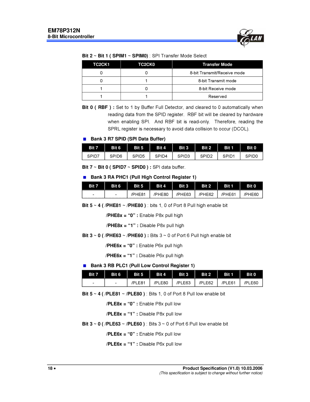
Bit 2 ~ Bit 1 ( SPIM1 ~ SPIM0) : SPI Transfer Mode Select
TC2CK1 | TC2CK0 |
| Transfer Mode |
|
|
|
|
0 | 0 |
| |
|
|
|
|
0 | 1 |
| |
|
|
|
|
1 | 0 |
| |
|
|
|
|
1 | 1 |
| Reserved |
|
|
|
|
Bit 0 ( RBF ) : Set to 1 by Buffer Full Detector, and cleared to 0 automatically when reading data from the SPID register. RBF bit will be cleared by hardware when enabling SPI. And RBF bit is
Bank 3 | R7 SPID (SPI Data Buffer) |
|
|
|
|
|
|
|
| ||||||
|
|
|
|
|
|
|
|
|
|
|
|
|
|
| |
Bit 7 |
|
| Bit 6 |
| Bit 5 |
| Bit 4 |
| Bit 3 |
|
| Bit 2 |
| Bit 1 | Bit 0 |
|
|
|
|
|
|
|
|
|
|
|
|
|
|
|
|
SPID7 |
|
| SPID6 |
| SPID5 |
| SPID4 |
| SPID3 |
|
| SPID2 |
| SPID1 | SPID0 |
|
|
|
|
|
|
|
|
|
|
|
|
|
|
| |
Bit 7 ~ Bit 0 ( SPID7 ~ SPID0 ) : SPI data buffer. |
|
|
|
| |||||||||||
Bank 3 | RA PHC1 (Pull High Control Register 1) |
|
|
|
| ||||||||||
Bit 7 |
| Bit 6 | Bit 5 | Bit 4 | Bit 3 |
- |
| - | /PHE81 | /PHE80 | /PHE63 |
|
|
|
|
|
|
Bit 2 | Bit 1 | Bit 0 |
/PHE62 /PHE61 /PHE60
Bit 5 ~ 4 ( /PHE81 ~ /PHE80 ) : bits 1, 0 of Port 8 Pull high enable bit /PHE8x = “0” : Enable P8x pull high
/PHE8x = “1” : Disable P8x pull high
Bit 3 ~ 0 ( /PHE63 ~ /PHE60 ) : Bits 3 ~ 0 of Port 6 Pull high enable bit /PHE6x = “0” : Enable P6x pull high
/PHE6x = “1” : Disable P6x pull high
Bank 3 RB PLC1 (Pull Low Control Register 1)
Bit 7 | Bit 6 | Bit 5 | Bit 4 |
|
|
|
|
Bit 3
Bit 2 | Bit 1 | Bit 0 |
-
-
/PLE81
/PLE80
/PLE63
/PLE62
/PLE61
/PLE60
Bit 5 ~ 4 ( /PLE81 ~ /PLE80 ) : Bits 1, 0 of Port 8 Pull low enable bit /PLE8x = “0” : Enable P8x pull low
/PLE8x = “1” : Disable P8x pull low
Bit 3 ~ 0 ( /PLE63 ~ /PLE60 ) : Bits 3 ~ 0 of Port 6 Pull low enable bit /PLE6x = “0” : Enable P6x pull low
/PLE6x = “1” : Disable P6x pull low
18 • | Product Specification (V1.0) 10.03.2006 |
(This specification is subject to change without further notice)