EM78P312N
8-Bit Microcontroller
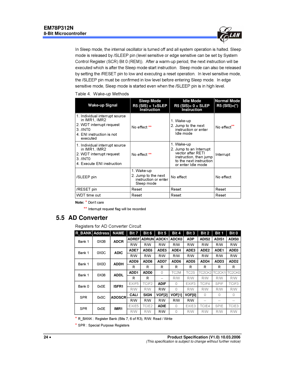
In Sleep mode, the internal oscillator is turned off and all system operation is halted. Sleep mode is released by /SLEEP pin (level sensitive or edge sensitive can be set by System Control Register (SCR) Bit 0 (REM)). After a
Table 4. Wake-up Methods
|
|
| Sleep Mode |
| Idle Mode |
| Normal Mode |
|
|
|
| R5 (SIS) = 1+SLEP |
| R5 (SIS)= 0 + SLEP |
| R5 (SIS)=(*) |
|
|
|
| Instruction |
| Instruction |
|
|
|
1. | Individual interrupt source |
|
|
|
|
|
|
|
| in IMR1, IMR2 |
|
|
| 1. |
|
|
|
2. WDT interrupt request |
| No effect ** | 2. Jump to the next |
| No effect** | |||
3. | /INT0 |
|
|
| instruction or enter |
|
|
|
4. | ENI instruction is not |
|
|
| Idle mode |
|
|
|
| executed |
|
|
|
|
|
|
|
1. | Individual interrupt source |
|
|
| 1. |
|
|
|
| in IMR1, IMR2 |
|
|
| 2. Jump to an Interrupt |
|
|
|
2. WDT interrupt request |
| No effect ** | vector after RETI |
| Interrupt | |||
| instruction, then jump |
| ||||||
3. | /INT0 |
|
|
| to the next instruction |
|
|
|
4. | Execute ENI instruction |
|
|
|
|
|
| |
|
|
| or enter Idle mode |
|
|
| ||
|
|
| 1. |
|
|
|
| |
/SLEEP pin |
| 2. Jump to the next | No effect |
| No effect | |||
| instruction or enter |
| ||||||
|
|
| Sleep mode |
|
|
|
| |
/RESET pin |
| Reset | Reset |
| Reset | |||
|
|
|
|
|
| |||
WDT time out |
| Reset | Reset |
| Reset | |||
|
|
|
|
|
|
|
|
|
Note: * Don’t care
**Interrupt request flag will be recorded
5.5AD Converter
Registers for AD Converter Circuit
R_BANK | Address |
| NAME |
| Bit 7 |
| Bit 6 |
| Bit 5 |
| Bit 4 |
| Bit 3 |
| Bit 2 |
| Bit 1 |
| Bit 0 |
Bank 1 | 0X0B |
| ADCR |
| ADREF |
| ADRUN |
| ADCK1 |
| ADCK0 |
| ADP |
| ADIS2 |
| ADIS1 |
| ADIS0 |
|
| R/W |
| R/W |
| R/W |
| R/W |
| R/W |
| R/W |
| R/W |
| R/W | |||
|
|
|
|
|
|
|
|
|
|
|
| ||||||||
Bank 1 | 0X0C |
| ADIC |
| ADE7 |
| ADE6 |
| ADE5 |
| ADE4 |
| ADE3 |
| ADE2 |
| ADE1 |
| ADE0 |
|
| R/W |
| R/W |
| R/W |
| R/W |
| R/W |
| R/W |
| R/W |
| R/W | |||
|
|
|
|
|
|
|
|
|
|
|
| ||||||||
Bank 1 | 0X0D |
| ADDH |
| ADD9 |
| ADD8 |
| ADD7 |
| ADD6 |
| ADD5 |
| ADD4 |
| ADD3 |
| ADD2 |
|
| R |
| R |
| R |
| R |
| R |
| R |
| R |
| R | |||
|
|
|
|
|
|
|
|
|
|
|
| ||||||||
Bank 1 | 0X08 |
| ADDL |
| ADD1 |
| ADD0 |
| 0 |
| TC2M |
| TC2S |
| TC2CK2 |
| TC2CK1 |
| TC2CK0 |
|
| R |
| R |
|
| R/W |
| R/W |
| R/W |
| R/W |
| R/W | ||||
|
|
|
|
|
|
|
|
|
|
|
| ||||||||
Bank 0 | 0x0E |
| ISFR1 |
| EXIF5 |
| TCIF2 |
| ADIF |
| 0 |
| EXIF3 |
| TCIF4 |
| SPIF |
| TCIF3 |
|
| R/W |
| R/W |
| R/W |
| 0 |
| R/W |
| R/W |
| R/W |
| R/W | |||
|
|
|
|
|
|
|
|
|
|
|
| ||||||||
SPR | 0x0C |
| ADOSCR |
| CALI |
| SIGN |
| VOF[2] |
| VOF[1] |
| VOF[0] |
| 0 |
| 0 |
| 0 |
|
| R/W |
| R/W |
| R/W |
| R/W |
| R/W |
|
|
| ||||||
|
|
|
|
|
|
|
|
|
|
|
| ||||||||
SPR | 0x0E |
| IMR1 |
| EXIE5 |
| TCIE2 |
| ADIE |
| 0 |
| EXIE3 |
| TCIE4 |
| SPIE |
| TCIE3 |
|
| R/W |
| R/W |
| R/W |
| 0 |
| R/W |
| R/W |
| R/W |
| R/W | |||
|
|
|
|
|
|
|
|
|
|
|
|
*R_BANK : Register Bank (Bits 7, 6 of R3), R/W: Read / Write
*SPR : Special Purpose Registers
24 • | Product Specification (V1.0) 10.03.2006 |
(This specification is subject to change without further notice)