EM78P312N
8-Bit Microcontroller
AD7 (P97) |
|
|
|
|
|
|
|
|
|
AD6 (P96) |
|
|
|
|
|
|
|
|
|
AD5 (P95) | 8 |
|
|
|
|
| VDD |
|
|
|
|
|
|
| VREF |
|
| ||
to 1 |
|
|
|
|
|
|
| ||
AD4 (P94) |
|
|
|
|
|
|
|
| |
Analog |
|
|
|
|
|
|
|
| |
|
|
|
|
| ADC | Power Down |
| ||
|
|
| (Successive Approximation) | Start to Convert |
|
| |||
AD3 (P93) | switch |
|
|
|
|
|
|
|
|
AD2 (P92) |
|
|
|
|
|
|
|
| |
| Fosc/4 |
|
|
|
|
|
|
| |
AD1 (P91) |
| 4 to 1 |
|
|
|
|
|
| |
| Fosc/16 |
|
|
|
|
|
| ||
AD0 (P90) |
| Fosc/32 | MUX |
|
|
|
|
|
|
|
|
|
|
|
|
|
|
| |
7 - 0 | 2 1 0 |
| 5 4 | 5 | 5 | 9 8 7 6 5 4 3 2 1 0 | 6 | 3 | 7 |
ADIC | ADCR | ADCR | ISFR1 |
| IMR1 | ADCR |
|
| |
|
|
|
|
| DATA BUS |
|
|
| |
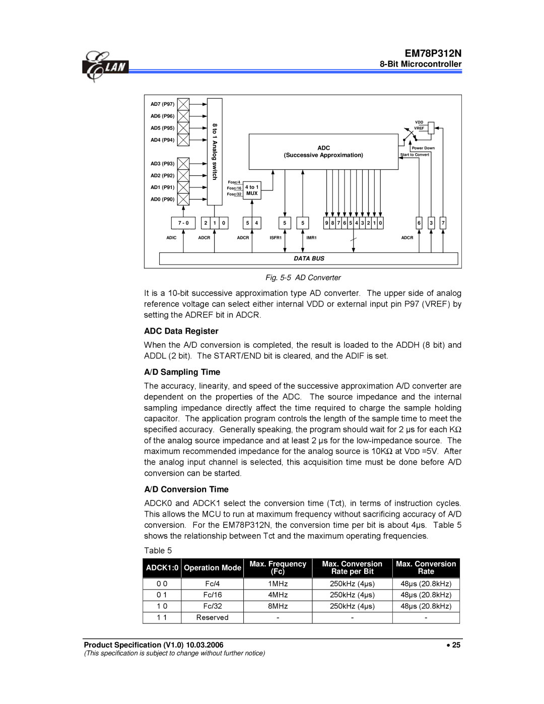
Fig. 5-5 AD Converter
It is a
ADC Data Register
When the A/D conversion is completed, the result is loaded to the ADDH (8 bit) and ADDL (2 bit). The START/END bit is cleared, and the ADIF is set.
A/D Sampling Time
The accuracy, linearity, and speed of the successive approximation A/D converter are dependent on the properties of the ADC. The source impedance and the internal sampling impedance directly affect the time required to charge the sample holding capacitor. The application program controls the length of the sample time to meet the specified accuracy. Generally speaking, the program should wait for 2 μs for each KΩ of the analog source impedance and at least 2 μs for the
A/D Conversion Time
ADCK0 and ADCK1 select the conversion time (Tct), in terms of instruction cycles. This allows the MCU to run at maximum frequency without sacrificing accuracy of A/D conversion. For the EM78P312N, the conversion time per bit is about 4μs. Table 5 shows the relationship between Tct and the maximum operating frequencies.
Table 5
| ADCK1:0 | Operation Mode |
| Max. Frequency |
| Max. Conversion |
| Max. Conversion |
|
|
|
|
|
| (Fc) |
| Rate per Bit |
| Rate |
|
|
| 0 0 | Fc/4 |
| 1MHz |
| 250kHz (4μs) |
| 48μs (20.8kHz) |
| |
| 0 1 | Fc/16 |
| 4MHz |
| 250kHz (4μs) |
| 48μs (20.8kHz) |
| |
| 1 0 | Fc/32 |
| 8MHz |
| 250kHz (4μs) |
| 48μs (20.8kHz) |
| |
| 1 1 | Reserved |
| - |
| - |
| - |
|
|
|
|
|
|
|
|
|
|
|
|
|
Product Specification (V1.0) 10.03.2006 |
|
|
|
|
| • 25 | ||||
(This specification is subject to change without further notice)