Intel® Server Board SDS2 | I/O Subsystem |
∙The scatter / gather mechanism supports both DMA and PIO IDE drives and ATAPI devices
∙Support for ATA and ATAPI, PIO Mode 0, 1, 2, 3, 4, DMA Mode 0, 1, 2, and Ultra DMA Mode 0, 1, 2, 3, 4, 5
∙The IDE drive transfer rate is capable of up to
4.5.3USB Interface
The CSB5 contains a USB controller and four USB hubs. The USB controller moves data between main memory and the four USB connectors.
The SDS2 Server Board provides a three external USB connector interface on the rear I/O. One additional USB is supported internally through a
4.5.4Compatibility Interrupt Control
The CSB5 provides the functionality of two 82C59 PIC devices for
4.5.5APIC
The CSB5 integrates a
4.5.6Power Management
One of the embedded functions of CSB5 is a power management controller. The SDS2 Server Board uses this to implement
4.5.7General Purpose Input and Output Pins
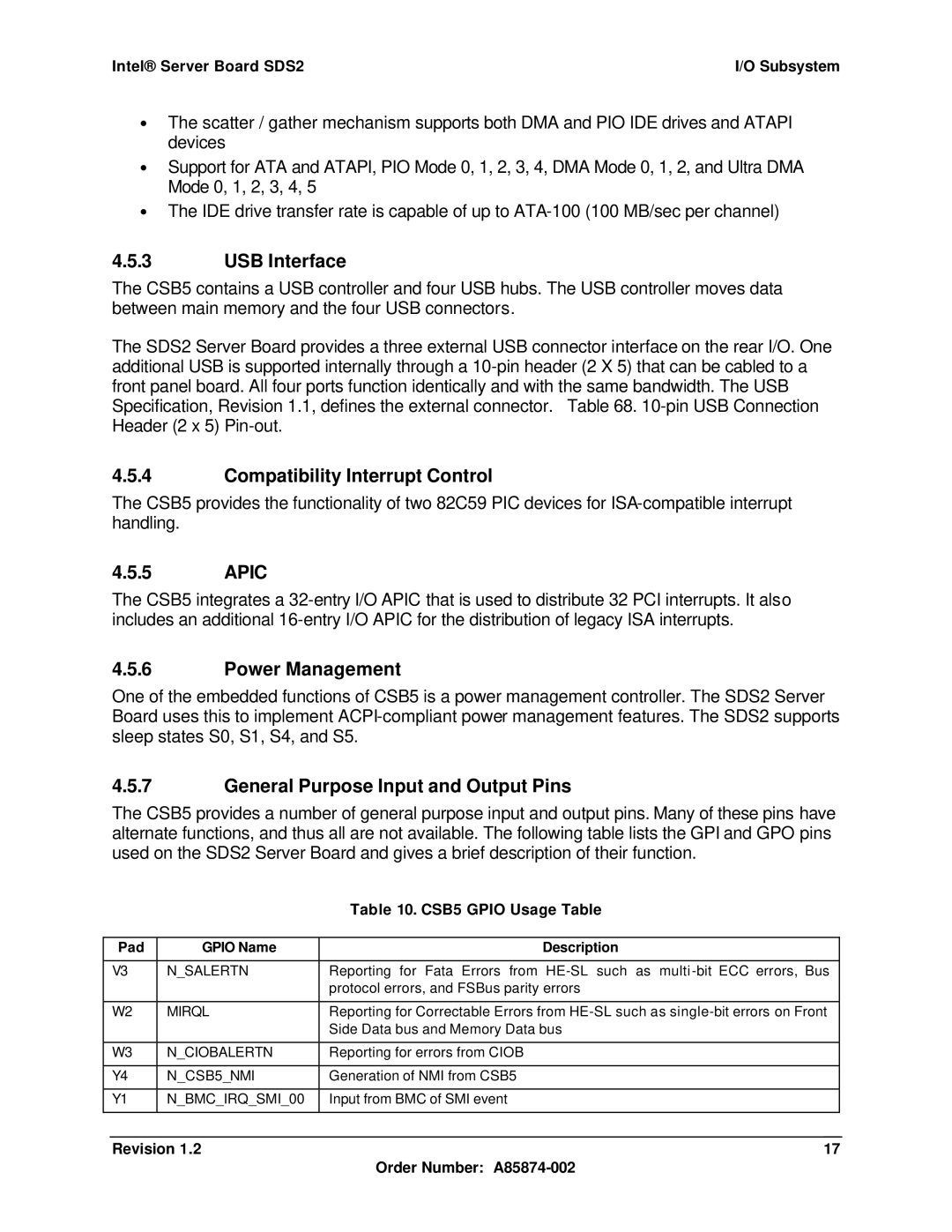
The CSB5 provides a number of general purpose input and output pins. Many of these pins have alternate functions, and thus all are not available. The following table lists the GPI and GPO pins used on the SDS2 Server Board and gives a brief description of their function.
|
|
| Table 10. CSB5 GPIO Usage Table | |
|
|
|
|
|
| Pad | GPIO Name | Description |
|
|
|
|
|
|
| V3 | N_SALERTN | Reporting for Fata Errors from |
|
|
|
| protocol errors, and FSBus parity errors |
|
|
|
|
|
|
| W2 | MIRQL | Reporting for Correctable Errors from |
|
|
|
| Side Data bus and Memory Data bus |
|
|
|
|
|
|
| W3 | N_CIOBALERTN | Reporting for errors from CIOB |
|
|
|
|
|
|
| Y4 | N_CSB5_NMI | Generation of NMI from CSB5 |
|
|
|
|
|
|
| Y1 | N_BMC_IRQ_SMI_00 | Input from BMC of SMI event |
|
|
|
|
|
|
|
|
|
|
|
| Revision 1.2 | 17 | ||
|
|
| Order Number: | |