Intel Server Board SDS2
Revision History Intel Server Board SDS2
Revision
Order Number A85874-002
Date Revision Modifications Number
Iii
Intel Server Board SDS2 Disclaimers
Table of Contents
Intel Server Board SDS2 Table of Contents
Revision Order Number A85874-002
Table of Contents Intel Server Board SDS2
101
102
106
Revision Vii Order Number A85874-002
124
Viii Revision Order Number A85874-002
Glossary
Reference Documents
Index
SDS2 Server Board Block Diagram
List of Figures Intel Server Board SDS2
List of Tables
Intel Server Board SDS2 List of Tables
List of Tables Intel Server Board SDS2
Xii Revision Order Number A85874-002
Revision Xiii Order Number A85874-002
This page intentionally left blank
Xiv Revision Order Number A85874-002
Introduction
Intel Server Board SDS2 Introduction
Architecture
Architecture Intel Server Board SDS2
Revision Order Number A85874-002
Processor and Chipset
Processors
Processor and Chipset Intel Server Board SDS2
SDS2 Intel Pentium III Processor Support Matrix
Intel Server Board SDS2 Processor and Chipset
SL5XL
Processor Voltage Regulator Module VRM
Memory Configuration
Memory Subsystem
Dimm Pair
Memory Dimm
Row
DIMM1A, DIMM1B DIMM2A, DIMM2B DIMM3A, DIMM3B
Chipset
2 I2C Bus
I2C Addresses for Dimm Slots
Device Address
1 CNB20HE-SL Champion North Bridge
PCI Bus P32-A I/O Subsystem
CIOB20 Champion I/O Bridge
3 CSB5 South Bridge
PCI Bus P64-B I/O Subsystem
PCI Bus P64-C I/O Subsystem
O Subsystem
PCI Subsystem
1 32-bit, 33-MHz PCI Subsystem
Device IDs Idsel
Subsystem Intel Server Board SDS2 P32-A Configuration IDs
2 64-bit, 66-MHz PCI Subsystem
1.2 P32-A Arbitration
P32-A Arbitration Connections
Intel Server Board SDS2 Subsystem P64-B Configuration IDs
P64-C Configuration IDs
2.2 P64-B Arbitration
2.3 P64-C Arbitration
Ultra160 Scsi
Video Controller
Video Modes
Zero Channel RAID ZCR Capable PCI Slot
Network Interface Controller NIC
Intel Server Board SDS2 Subsystem Video Modes
NIC Connector and Status LEDs
CSB5 South Bridge PCI-to-LPC Bridge, IDE, USB
PCI Bus Interface
PCI Bus Master IDE Interface
Power Management
General Purpose Input and Output Pins
USB Interface
Compatibility Interrupt Control
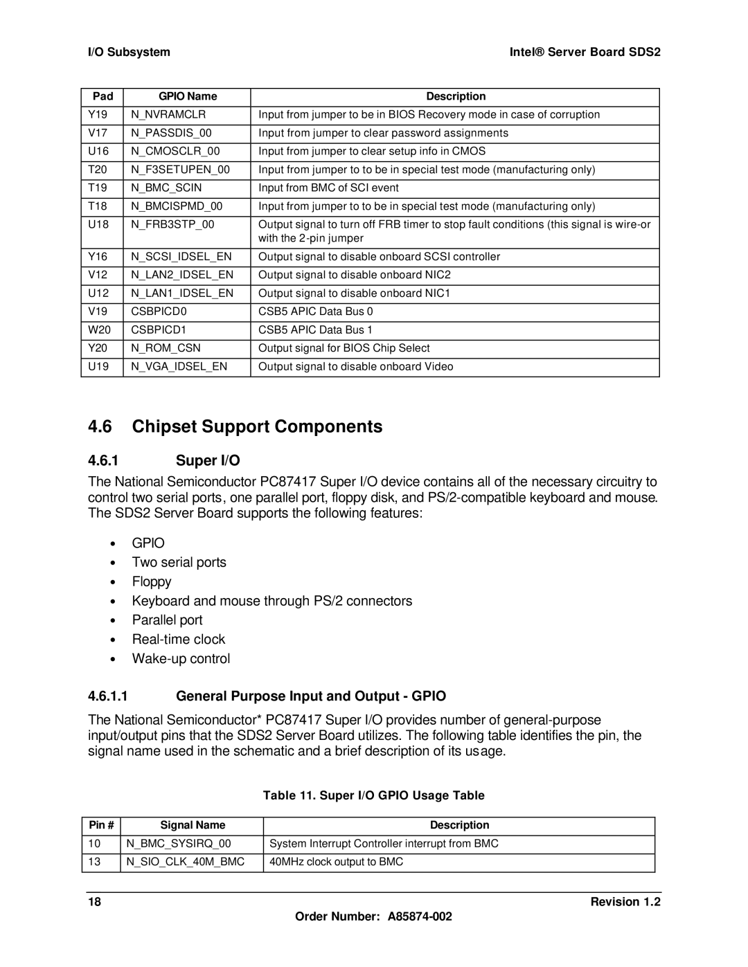
Pin # Signal Name Description
Chipset Support Components
Super I/O
General Purpose Input and Output Gpio
Serial Ports
Floppy
Keyboard and Mouse
Parallel Port
Bios Flash
Interrupt Routing
Legacy Interrupt Routing
Legacy Interrupt Routing
IRQ Scan for Pciirq
Apic Interrupt Routing
Serialized IRQ Support
Ioapic
SCAN2 INT
SCAN0 Ioapic
PCIIRQ0
Super I/O
Serialized IRQ Interface PCI IRQ Serializer
CSB5 Interrupt Routing
Slot
Server Management
Intel Server Board SDS2 Server Management
Server Management Intel Server Board SDS2
Baseboard
ADM1026 Input Definition
Pin Signal Name Description
Sahalee Baseboard Management Controller
Sahalee Input Definition
Temperature Sensors
Temperature Sensor Description Resolution Accuracy
Fault Resilient Booting
NFAN6SENSEP
Nmemalertl
Nbmcsecuremode
System Reset Control
Power-up Reset
Hard Reset
Soft Reset
Intel Server Board SDS2 Server Management Ipmb Bus Devices
Private I2C Bus 1 Devices
Private I2C Bus 2 Devices
Private I2C Bus 3 Devices
Error Reporting
Error Sources and Types
PCI Bus Errors
Intel Pentium III Processor Bus Errors
AC Link Mode
Memory Bus Errors
Acpi
ID LED
Setup Utility F2 can change the AC link mode settings
Bios
System Bios
Logging Format Conventions
Bios Error Handling
Handling and Logging System Errors
Bios Generated SEL Errors
Sensor Sensor Type Number Specific Event Code Offset
PCI Serr
PCI Perr
PCI Bus Error
Intel Pentium III Processor Bus Error
Event Request Message Event Data Field Contents
SMI Handler
Firmware BMC
Name
Sensor Type Triggers Event Reading Offset
BB Vbat
Lvds Scsi
OEM C7h 01h Temp Tach Fan 48h Fan 04h Threshold 49h
Ierr FRB1
FRB2 FRB3
Timestamp Clock
Error Messages and Error Codes
ASF Progress Codes
Post Codes
Port-80h Code Definition
Standard Bios Post Codes
Bios
Bios
Recovery Bios Post Codes
Beeps Reason
Post Error Codes and Messages
Post Error Messages and Codes
Code Error Message Failure Description
Cmos
Reason for Beep
Baseboard Management Controller BMC Beep Code Generation
BMC Beep Codes
Setup Utility
Configuration Utilities Overview
Setup Utility Operation
Setup Utility Screen
Entering Setup Utility
Keyboard Command Bar
Key Option Description
ESC
Menu Selection Bar
Main Menu Selections
Cdrom
Primary Master and Slave IDE Submenu Selections
Auto
Standard
Processor Settings Submenu Selections
Not Installed
Memory Configuration Menu Selections
Advanced Menu Selections
PCI Configuration Menu Selections
On-board Scsi and LAN Submenu Selections
On-board VGA Submenu Selections
PCI slot Submenu Selections
Bios
O Device/Peripheral Configuration Submenu Selections
3F8h
2F8h
EPP
Security Menu Selections
Advanced Chipset Controller Submenu Selections
PCI Device Submenu Selections
Hours
Server Menu Selections
Normal
Disable Immediately
System Management Submenu Selections
BMC IRQ
IRQ5 IRQ10
Boot Device Priority Selections
Boot Priority Device Description
Console Redirection Submenu Selections
9600
Hard Drive Selections
Removable Drive Selections
Exit Menu Selections
Option Description
Flash Update Utility
Loading the System Bios
Cmos Memory Definition
Clearing Cmos
Recovery Mode
Performing Bios Recovery
User Binary Area
Language Area
Bios
Clock/Voltage Generation and Distribution
Clock
CPU HE-SL
Voltage
Supply
Power Distribution Board Connector
Connections
Memory Module Connector
Dimm Connector Pin-out
Intel Server Board SDS2 Connections
Pin Front Back
Icmb Connector
OEM Ipmb Connector
Scsi Hsbp Ipmb Connector
System Management Headers
Front Panel Header
Front Panel 34-Pin Header Pin-out
KEY
I2C SDA
PCI Slot Connector
Bit 5 V PCI Slot Pin-out
64-bit 3.3V PCI Slot Pin-out
Pin Side B Side a
TDO TDI INTA# INTB# INTC# INTD# PRSNT1# RSV
PRSNT2# RSV
M66EN
PAR64
I/O Connectors
VGA Connector
Scsi Connector
VGA Connector Pin-out
Signal Name Connector Contact Number
NIC Connectors
RJ-45 Connector Pin-out
IDE Connector
Universal Serial Bus USB Connectors
IDE 40-pin Connector Pin-out
Txdp Rxdp Txdm Rxdm
Floppy Connector
Pin USB Connection Header 2 x 5 Pin-out
Serial Port Connector
DB9 Serial Port Pin-out
DB25 Parallel Port Pin-out
Keyboard and Mouse Connector
Parallel Port
External Scsi Activity LED Input Signal Connector
Miscellaneous Headers
Fan Headers
Chassis Intrusion
Connector Manufacturers and Part Numbers
Server Board Connector Manufacturer Part Numbers
Rear I/O Panel
CN Numbers Qty Manufacturer Mfg Functional Description
Jumpers Intel Server Board SDS2
System Configuration Jumpers
Jumpers
SDS2 Configuration Jumpers
Intel Server Board SDS2 Jumpers
RSV
System Configuration Jumper Options
Bios
CN59 CPU Frequency Select Jumper Settings
CPU Frequency Select Jumper Options
Performing Cmos Clear, Bios Recovery, and BMC Force Update
Performing Bios Recovery Boot
Jumper Pins Default Operation
Performing Cmos Clear
Performing BMC Force Update
Electrical and Thermal Specifications
Power Consumption
Absolute Maximum Ratings
Absolute Maximum Ratings
Power Supply Specification
Power Timing
SDS2 Power Supply Specification
Voltage Timing Parameters
Page
100 Revision Order Number A85874-002
Estimateded Server Board Mtbf
Estimated SDS2 Server Board Mtbf Turn On/Off Timing
Mechanical Specifications
Intel Server Board SDS2 Mechanical Specifications
Safety Regulations
Regulatory and Integration Information
Regulatory Compliance
EMC Regulations
Revision 103 Order Number A85874-002
Installation Instructions
Ensure EMC
Place Battery Marking on Computer
Ensure Host Computer and Accessory Module Certifications
Prevent Power Supply Overload
Installation Precautions
Icmb External Cable Connectors
Use Only for Intended Applications
External Icmb Cable Information
Errata Listing
Summary Errata Table
Errata Listing Intel Server Board SDS2
Errata Summary
Intel Server Board SDS2 Errata Listing
Revision 107 Order Number A85874-002
108 Revision Order Number A85874-002
Revision 109 Order Number A85874-002
Intel Server Board SDS2 CD-ROM issues
110 Revision Order Number A85874-002
Revision 111 Order Number A85874-002
112 Revision Order Number A85874-002
High resolution video modes do not work correctly
Mode Support Comments
Lower performance with CAS Latency 2 memory
Revision 113 Order Number A85874-002
Novell NetWare* v .0 does not install on SDS2
114 Revision Order Number A85874-002
SDS2 0B71 System Temperature out of the range Post message
Revision 115 Order Number A85874-002
SDS2 0B75 System Voltage out of the range Post message
116 Revision Order Number A85874-002
Recommendation for SDS2 rubber bumper installation
Revision 117 Order Number A85874-002
118 Revision Order Number A85874-002
Placing the Rubber Bumper in the Chassis
Revision 119 Order Number A85874-002
120 Revision Order Number A85874-002
Boot to service partition via modem fails
Secondary IDE References Added To Documentation for FAB
Bootable CD will not boot if inserted during Option ROM scan
Revision 121 Order Number A85874-002
122 Revision Order Number A85874-002
Revision 123 Order Number A85874-002
Can Not Change Bios Setup IDE Options Using Enter Key
Status Will Not Fix
124 Revision Order Number A85874-002
SDS2 PCI slot current levels supported by the 5V rail
Revision 125 Order Number A85874-002
126 Revision Order Number A85874-002
Term Definition
Glossary Intel Server Board SDS2
Reference Documents
Index
Index Intel Server Board SDS2
Get SDR Time command, 43 Get SEL Time command, 43 GPI pin
NPWRGD+00
RevisionIII Order Number A85874-002
Index Intel Server Board SDS2
RevisionV Order Number A85874-002