User’s Guide
Important Notice
Basic Registers
Introduction to the MSC1210
MSC1210 Memory Organization
Serial Communication
Addressing Modes
System Timing
Pulse Width Modulator/Tone Generator
Analog-to-Digital Converter
Serial Peripheral Interface SPI
Additional MSC1210 Hardware
Additional Resource
Boot ROM Routines
Additional Features in the MSC1210 Compared to
Clock Timing Diagram
Instruction-Set Quick-Reference Guide
SPI/PWM/Flash Write Timing System Timing Interrupt Control
16−1
Pin Descriptions of the MSC1210
14−2
Chapter
−1. MSC1210 Block Diagram
MSC1210 Description
−2. Pin Configuration of the MSC1210
MSC1210 Pin-Out
−1. Pin Descriptions of the MSC1210
Pin # Name Description
−1 Pin Descriptions of the MSC1210
Pin # Name Description
1 I/O Ports P0, P1, P2, and P3
AD7
Port
Port
Oscillator Inputs XTAL1 and XTAL2
Program Store Enable Psen
Reset Line RST
Address Latch Enable ALE
External Access EA
Enhanced 8051 Core
−3. MSC1210 Timing Compared to Standard 8051 Timing
High Performance Analog Functions
Family Device Compatibility
Flash Memory
High-Performance Peripherals
Description Program Memory Data Memory Internal RAM
Description
Program Memory
−1. Program and Data Memory Size
MSC1210Y2 MSC1210Y3 MSC1210Y4 MSC1210Y5
On-Chip Extended Static RAM Sram
Data Memory
−2. Program and Data Memory Addresses
On-Chip Flash Data Memory
External Data Memory
Internal RAM
−2. MSC1210 Memory Map Register Bank
Stack
Register Banks
Bit Memory
Or execute
Special Function Register SFR Memory
Defines the MSC1210 SFRs
−1. SFR Names and Addresses
SCON0
Referencing SFRs
Referencing Bits of SFRs
Bit−Addressable SFRs
SFR Types
SFR Definitions
SFR Definitions
SFR Definitions
SFR Definitions
Can be generated automatically by the MSC1210
P0DDRL/P0DDRH Port 0 Data Direction Low/High Byte, Addresses
GCL/GCM/GCH Gain Low/Middle/High Byte, Addresses D4H/D5H/D6H
SFR Definitions
SFR Definitions
SFR Definitions
Describes the basic register functions of the MSC1210 ADC
Accumulator
Registers
Register
Program Counter PC
Data Pointer DPTR0/DPTR1
Stack Pointer SP
Describes the various addressing modes of the MSC1210
−1. MSC1210 Addressing Modes
Mode Example
Immediate Addressing
Direct Addressing
Indirect Addressing
External Direct Addressing
Movx A,@DPTR Movx @DPTR,A
External Indirect Addressing
Code Indirect Adressing
Describes the program flow of the MSC1210 ADC
Conditional Branching
Direct Jumps
Consider the example
Interrupts
Direct Calls
Returns From Routines
Description System Timers Startup Timing
−1. Standard 8051 Timing
System Timing
System Timers
−2. MSC1210 Timing Chain and Clock Control
Microseconds Timer
Milliseconds Timer
−4. System Timing Interrupt Control
One Hundred Millisecond Clock
Startup Timing
Normal-Mode Power-On Reset Timing
Flash Programming Mode Power-On Reset Timing
Symbol Parameter Min Max Unit
Psen
Describes the timers of the MSC1210 ADC
How Long Does a Timer Take to Count?
How Does a Timer Count?
Using Timers to Measure Time
Movx Duration SYS CLKs At 12MHz
RD or WR Strobe
Width Width ∝s
SFR Name Description SFR Address Bit Addressable?
Timer SFRs
−1. Timer Conrol SFRs
Tmod SFR
Mode
−2. Timer Modes and Usage
TxM1 TxM0 Timer Description of Timer Mode
Cycle
−3. Example of 8-Bit Auto-Reload
Instruction
−4. Tcon 88 H SFR
Bit Name Bit Address Explanation of Function Timer
Tcon SFR
Initializing a Timer
Reading the Timer
Detecting Timer Overflow
Timing the Length of Events
Using Timers as Event Counters
Using Timer
1 T2CON SFR
Timer 2 in Auto-Reload Mode
Timer 2 in Capture Mode
Timer 2 as a Baud Rate Generator
Describes serial communication using the MSC1210 ADC
Description
Setting the Serial Port Mode
Function Length Period
−1. SM0 and SM1 Function Definitions
Mode
Serial Mode 0 Synchronous Half-Duplex
High four bits bits 4 through 7 are configuration bits
−2. Serial Port Mode 0 Receive Timing-High Speed Operation
Serial Mode 1 Asynchronous Full-Duplex
−3. Serial Port Mode 1 Transmit Timing
BaudRate + Timer2Overflow
−2. Common Baud Rates Using Timer
BaudRate + 32 @ Timer1Overflow
BaudRate + 12 @ 256 * TH1
Rcap 2H Rcap 2L +
−3. Common Baud Rates Using Timer
Serial Mode 2 Asynchronous Full-Duplex
Baud Rate RCAP2HRCAP2L @ 11.0592MHz f OSC
−6. Serial Port 0 Mode 2 Receive Timing
BaudRate + 2SMOD @ fOSC
Serial Mode 3 Asynchronous Full-Duplex
−7. Serial Port 0 Mode 3 Transmit Timing
Setting the Serial Port Mode
TH1 = 256 − Crystal / 192 / Baud
Setting the Serial Port Baud Rate
−4. Mode 0 Commonly Used Baud Rates
Baud Rate
−5. Baud Rate Settings for Timer
Desired Baud
Baud Rate 33MHz clk 25MHz clk 11.0592MHz clk Kb/s
−6. Baud Rate Settings for Timer
Writing to the Serial Port
Reading the Serial Port
Describes the interrupts of the MSC1210 ADC
JNB TF0,SKIPTOGGLE
−1.Interrupt Sources
Interrupt/Event Addr Priority Flag Enable Priority Control
Events That Can Trigger Interrupts
10-4
−3.EICON D8 H SFR
Enabling Interrupts
−2.IE A8 H SFR
−4.EIE E8 H SFR
Polling Sequence
−6.EIP F8 H SFR
Interrupt Priorities
−5.IP B8 H SFR
Interrupt Triggering
Exiting Interrupts
External Interrupts
Types of Interrupts
Serial Interrupts
−7.EXIF 91 H SFR
Bit Name Explanation of Function
Auxiliary Interrupts
Timer Interrupts
Watchdog Interrupt
Aux Interrupt Type Method to Clear Interrupt
−8.Clearing Auxiliary Interrupts
−9.AIE A6 H SFR
Bit Name Explanation of Function Clear Interrupt
−10. Aistat A7 H SFR
−11. PAI A5 H SFR
−12. PPI Bits of PAI SFR
PAIx Bits Explanation of Interrupt/Event
Waking Up from Idle Mode
−13. EWU C6 H SFR
Register Protection
Push PSW
Push R0 Error − Invalid instruction
Common Problems with Interrupts
PWM Generator 11-5
Description 11-2
Tone Generator 11-3
−1. Block Diagram
Tone Generator
ToneFrequency +1
−3. Timing Diagram of Tone Generator in Staircase Mode
Tone Generator Waveforms
Duty Cycle = PWM Period +1 − PWM Duty/PWM Period +1
PWM Generator
−1. PWM Polarity Conditions
Condition Duty Cycle
−5. Timing Diagram of a PWM Waveform
This can be expressed in code as
Example of PWM Tone Generation
−2. Configuring the PWM for Tone Generation
Stmt ‘C’ Source Code Assembly Source Code
−3. Statement Explanations
Example of PWM Tone Generation Idling
Explanation
−4. Configuring the PWM for Tone Generation with PWM Idling
−5. Statement Explanations
Example of Updating PWM
−6. PWM Timing
11-12
PGA DAC
12-10
−1. MSC1210 Architecture
−2. Input Multiplexer Configuration
Input Multiplexer
Positive Input
Negative Input
Temperature Sensor
12-6
Burnout Current Sources
MSB
@ 10
Input Buffer
Analog Input
ACLKFrequency
−1.PGA Settings
Programmable Gain Amplifier PGA
Offset DAC
Modulator
Calibration
−2.Calibration Mode Control Bits
Calibration Mode
Digital Filter
−4. Filter Step Responses
−5. Filter Frequency Responses
−4.Output Data Rate and Channel Rate
Multiplexing Channels
−3.Filter Settling
Samples to Discard Filter
Voltage Reference
−5.Output Data Rate and Channel Rate 10x faster
Summation/Shifter Register
Source
Summation Count
Shift Summation Count
Manual Summation Mode
ADC Summation Mode
Manual Shift Divide Mode
ADC Summation with Shift Divide Mode
Interrupt-Driven ADC Sampling
Analog-to-Digital Converter 12-21
Syncronizing Multiple MSC1210 Devices
Analog-to-Digital Converter 12-23
PT100
Ratiometric Measurements
ADC Result + V REF
ADC Result + R REF @ I OUT
Differential Vref
12-26
SPI System Errors 13-6
Clock Phase and Polarity Controls 13-4
SPI Signals 13-5
Description 13-2
−1. SPI block diagram
Functional Description
−2. SPI Clock/Data Timing
Clock Phase and Polarity Controls
Master Out Slave
SPI Signals
Master In Slave Out
Serial Clock
SPI System Errors
−3. SPI Reset State
Data Transfers
13-8
Fifo Operation
−4. SPI Fifo Operation
Code Examples
SPI Master Transfer in Fifo Mode using Interrupts
13-12
Low-Voltage Detect 14-2
Watchdog Timer 14-4
Description 14-2
−1. Brownout Reset and Low-Voltage Detection
Low-Voltage Detect
−1.Typical Sub-Circuit Current Consumption
Power Supply
−2.Comparator Specification
−3.Band Gap Parameters
Watchdog Timer
Watchdog Timer Hardware Configuration
Enabling Watchdog Timer
Watchdog Timer
Resetting the Watchdog Timer
Disabling Watchdog Timer
Watchdog Timeout/Activation
Advanced Flash Memory 15-6
Hardware Configuration 15-2
Power Optimization 15-9
Breakpoint Generator 15-7
Hardware Configuration
Hardware Configuration Registers
Hardware Configuration Register 0 HCR0
DFSEL2/1/0 Amount of Flash Data Memory
Hardware Configuration Register 1 HCR1
Hardware Configuration Memory
Accessing Configuration Memory in a User Program
Write Protecting Flash Program Memory
Updating Interrupts with Reset Sector Lock
Advanced Flash Memory
Configuring Breakpoints
Breakpoint Generator
Breakpoint Auxiliary Interrupt
Disabling a Breakpoint
Power Optimization
Flash Memory as Data Memory
Advanced Topics 15-11
Advanced Topics and Other Information
Describes the 8052 Assembly Language
Syntax
Label and instruction
Number Bases
Expressions
−1.Order of Precedence for Mathematical Operators
Operator Precedence
Characters and Character Strings
Order Operator
Changing Program Flow LJMP, SJMP, Ajmp
Ljmp LABEL3
Subroutines LCALL, ACALL, RET
Register Assignment MOV
MOV DestinationRegister,SourceValue
MOV R2,R1 Invalid
MOV @R0,A
Incrementing and Decrementing Registers INC, DEC
Program Loops Djnz
Setting, Clearing, and Moving Bits SETB, CLR, CPL, MOV
16-14
Bit-Based Decisions and Branching JB, JBC, JNB, JC, JNC
Value Comparison Cjne
Lcall Debouncekey
Less Than and Greater Than Comparison Cjne
Checkless JC Aisless
Zero and Non-Zero Decisions JZ/JNZ
Performing Additions ADD, Addc
Performing Additions ADD, Addc
Performing Subtractions Subb
Performing Multiplication MUL
Performing Division DIV
Shifting Bits RR, RRC, RL, RLC
−1. Rotate Operations
−3.Results of ORL
Bit-Wise Logical Instructions ANL, ORL, XRL
−2.Results of ANL
−4.Results of XRL
Assembly Language 16-25
Exchanging Register Values XCH
Swapping Accumulator Nibbles Swap
Adjusting Accumulator for BCD Addition DA
Using the Stack PUSH/POP
Assembly Language 16-29
Setting the Data Pointer Dptr MOV Dptr
Reading and Writing External RAM/Data Memory Movx
Reading Code Memory/Tables Movc
Lcall SUB
SUB INC a
Using Jump Tables JMP @A+DPTR
Describes the Keil simulator and its functions
17-2
Keil Simulator 17-3
Timers
−1. Timer/Counter 0 − Mode
Timer 0 & 1 Example
−2. Timer/Counter
−4. Timer/Counter 1 Mode
Keil Simulator 17-7
17-8
Keil Simulator 17-9
17-10
Register Bit Toggle Box Name
Timer
−1.Timer/Counter 2 Control Bits
−7. Status of Watchdog Peripheral
Watchdog Reset Facility Example
17-14
Keil Simulator 17-15
System Timer
Clock Control
Analog-to-Digital Converter
−8. Analog−to−Digital Converter Peripheral
−9. Error Message
Summation/Shifter
−10. Accumulator/Shifter Peripheral
17.8.1 ADC/Summation/Shifter Example
17-22
Keil Simulator 17-23
17-24
Keil Simulator 17-25
17-26
Keil Simulator 17-27
−11. summation/Shifter Peripheral
Keil Simulator 17-29
−13. List Box for the Interrupt Peripheral
−14. Parallel Port 0 Contents Display Window
Ports
Serial Peripheral Interface SPI
−16. SPI Peripheral Window
Keil Simulator 17-33
SPI Sample Code
Keil Simulator 17-35
Serial Peripheral Interface SPI
Keil Simulator 17-37
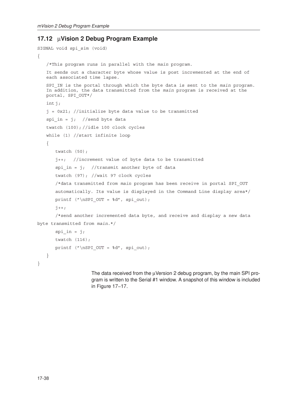
17.12 ∝Vision 2 Debug Program Example
−17. Keil Debugger
Serial Port I/O
−18. Serial Channel 0 Communication Peripheral
17-42
BaudRate + fOSC @
Transmit Block Baud Rate Computation
BaudRate + fOSC
Receive Block Baud Rate Computation
−19. Clock Control Peripheral
Additional Resource
Appendix a
Topic
Additional Features in the MSC1210 Compared to
Appendix B
MSC1210 Timing Chain and Clock Control Diagram
Figure B−1. MSC1210 Timing Chain and Clock Control
Appendix C
Table C−1. Boot ROM Routines
Address Routine Declarations Description
Boot ROM Routines
Page
Appendix D
8052 Instruction-Set Quick-Reference Guide
JB bitAddr,relAddr Ajmp pg1Addr
Appendix E
Description Instruction Set
Description
Absolute Call within 2k Block
8052 Instruction Set
Acall
Acall codeAddress
ADD A,operand
ADD, Addc
Add Value, Add Value with Carry
Ajmp codeAddress
Ajmp
Absolute Jump within 2k Block
ANL operand1,operand2
ANL
Bitwise
Clear Register
Compare and Jump if Not Equal
CLR
Cjne operand1,operand2,reladdr
Complement Register
Decimal Adjust Accumulator
CPL
CPL operand
DEC register
Decrementing the value causes it to reset to 255 0xFFH
Carry flag is not set when the value rolls over from 0 to
See also INC, Subb
Decrement and Jump if Not Zero
Djnz register,relAddr
INC register
INC
Increment Reister
Jump if Bit Set and Clear Bit
Jump if Bit Set
JBC
Jump if Carry Set
JNC
JMP
JNB
Ljmp
JNZ
Lcall
MOV bit1,bit2
MOV operand1, operand2
Not affected See also MOVC, MOVX, XCH, XCHD, PUSH, POP
MOV operand1,operand2
MOV
Move into/out of Internal RAM
Movx
MOV Dptr
Movc
NOP
MUL
Multiply Accumulator by B
No Operation
Syntax ORL operand1,operand2
ORL
Bitwise or
Push
POP
Pop Value from Stack
Push Value onto Stack
Reti
RET
Return from Subroutine
Return from Interrupt
Setb
RLC
RRC
Subb
Sjmp
Short Jump
Subtract from Accumulator with Borrow
Xchd
Swap
XCH
XRL
Bitwise Exclusive or
Undefined
Instructions OpCode Bytes Cycles Flags ??? 0xA5
Appendix F
EX2-External 2 Interrupt Enable
Enable Interrupt Control Eicon
Extended Interrupt Enable EIE
Bit Addressable SFRs alphabetical
Interrupt Enable IE
Extended Interrupt Priority EIP
Interrupt Priority IP
Port 0 P0
Port 1 P1
Port 2 P2
Port 3 P3
Program Status Word PSW
Register Bank Register Bank Addresses
Serial Mode Description Baud
Serial Control Scon
Timer Control Tcon
Tcon
Timer 2 Control T2CON
T2CON
Appendix G
SFR/Address Cross-Reference
SFR Name Description SFR Address Hex
SFRs/Address Cross-Reference Guide alphabetical
Spircon