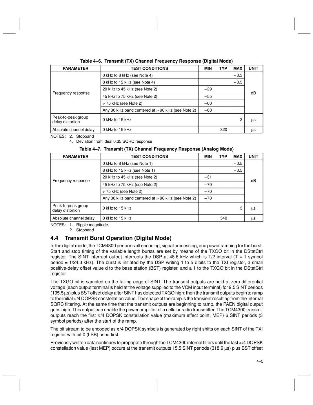
Table 4±6. Transmit (TX) Channel Frequency Response (Digital Mode)
PARAMETER | TEST CONDITIONS | MIN TYP MAX | UNIT | |
|
|
|
| |
| 0 kHz to 8 kHz (see Note 4) | ± 0.3 |
| |
|
|
|
| |
| 8 kHz to 15 kHz (see Note 4) | ± 0.5 |
| |
|
|
|
| |
Frequency response | 20 kHz to 45 kHz (see Note 2) | ± 29 | dB | |
|
| |||
45 kHz to 75 kHz (see Note 2) | ± 55 | |||
|
| |||
|
|
|
| |
| > 75 kHz (see Note 2) | ± 60 |
| |
|
|
|
| |
| Any 30 kHz band centered at > 90 kHz (see Note 2) | ± 60 |
| |
|
|
|
| |
0 kHz to 15 kHz | 3 | μs | ||
delay distortion | ||||
|
|
| ||
|
|
|
| |
Absolute channel delay | 0 kHz to 15 kHz | 320 | μs | |
|
|
|
| |
NOTES: 2. Stopband |
|
|
|
4. Deviation from ideal 0.35 SQRC response
Table 4±7. Transmit (TX) Channel Frequency Response (Analog Mode)
PARAMETER | TEST CONDITIONS | MIN TYP MAX | UNIT | |
|
|
|
| |
| 0 kHz to 8 kHz (see Note 1) | ± 0.5 |
| |
|
|
|
| |
| 8 kHz to 15 kHz (see Note 1) | ± 0.5 |
| |
|
|
|
| |
Frequency response | 20 kHz to 45 kHz (see Note 2) | ± 31 | dB | |
|
| |||
45 kHz to 75 kHz (see Note 2) | ± 70 | |||
|
| |||
|
|
|
| |
| > 75 kHz (see Note 2) | ± 70 |
| |
|
|
|
| |
| Any 30 kHz band centered at > 90 kHz (see Note 2) | ± 70 |
| |
|
|
|
| |
0 kHz to 15 kHz | 3 | μs | ||
delay distortion | ||||
|
|
| ||
|
|
|
| |
Absolute channel delay | 0 kHz to 15 kHz | 540 | μs | |
|
|
|
| |
NOTES: 1. Ripple magnitude |
|
| ||
2.Stopband
4.4Transmit Burst Operation (Digital Mode)
In the digital mode, the TCM4300 performs all encoding, signal processing, and power ramping for the burst. Start and stop timing of the variable length bursts are set by means of the TXGO bit in the DStatCtrl register. The SINT interrupt output interrupts the DSP at 48.6 kHz which is T/2 interval (T = 1 symbol period = 1/24.3 kHz). The burst is initiated by the DSP writing 1 to 5 dibits to the TXI register, a small
The TXGO bit is sampled on the falling edge of SINT. The transmit outputs are held at zero differential voltage (each output terminal is held at the voltage supplied to the VCM input terminal) for 9.5 SINT periods (195.5 μs) plus BST offset delay after SINT has detected TXGO high; then the transmit outputs begin to ramp to the initial π /4 DQPSK constellation value. The shape of the ramp is the transient resulting from the internal SQRC filtering. At the same time that the transmit outputs are beginning to ramp, the PAEN digital output goes high. This output can enable the power amplifier of a cellular radio transmitter. The TCM4300 transmit outputs reach the first π /4 DQPSK constellation value (maximum effect point, MEP) 6 SINT periods (3 symbol periods) after the start of the ramp.
The bit stream to be encoded as π /4 DQPSK symbols is generated by right shifts on each SINT of the TXI register with bit 0 (LSB) used first.
Previously written data continues to propagate through the TCM4300 internal filters until the last π /4 DQPSK constellation value (last MEP) occurs at the transmit outputs 15.5 SINT periods (318.9 μs) plus BST offset
4±5