Data Manual
SLWS010F
TCM4300 Data Manual
Important Notice
Contents
Mechanical Data ±1
List of Illustrations
List of Tables
Introduction
Features
TCM4300 Functional Block Diagram
Fmrxen
Pin Assignments
PZ Package TOP View
VSS
Terminal Description Name
Terminal Functions
Dvss
Dsprw
Dspstrbl
Dvdd
Mcrw
Mcds
MTS1
Mclkin
Syndta
Scen
Sint
Synclk
Derating Factor
Power Rating Above TA = 25C
Dissipation Rating Table
Package
Power Consumption
Reference Characteristics
Recommended Operating Conditions
Parameter Test Conditions MIN TYP MAX Unit
Terminal Impedance
RXIP, RXIN, RXQP, and Rxqn Inputs Avdd = 3 V, 4.5 V, 5
Function MIN TYP² MAX Unit
Transmit I and Q Channel Outputs
Auxiliary D/A Converters
Parameter MIN TYP MAX Unit
Nominal LSB Nominal Output Voltage
RSSI/Battery A/D Converter
Auxiliary D/A Converters Slope AGC, AFC, Pwrcont
Auxiliary D/A Converters Slope Lcdcontr
Transmit TX Channel Frequency Response Digital Mode
Transmit TX Channel Frequency Response Analog Mode
Page
Mclkout Timing Requirements see ±1 and Note
Mclkout
VOH VOL
MCA4±MCA0 MCD7±MCD0 Mccsh Mccsl
Parameter Alternate MIN MAX Unit
Mcds
Mcrw
MCA4±MCA0
Parameter Alternate MIN MAX Unit Symbol
MCA4±MCA0 MCD7±MCD0
Twdho
MCA0±MCA4 MCD0±MCD7 Mccsh Mccsl
Motorola 16-Bit Read Cycle, MTS 10 =
MCA0±MCA4
MCD0±MCD7 Mccsh Mccsl
Mcrw MCA0±MCA4
10% ThR / W ThWA
Dspa Dspd
Dspcsl
Dspstrbl
Dsprw
±11. TCM4300 to DSP Interface Write Cycle
±12
Data Transfer
±1. TCM4300 Receive Channel Control Signals
Control Signal Analog Mode Digital Mode
Mode Fmvox Iqrxen Fmrxen
±2. RXIP, RXIN, RXQP, and Rxqn Inputs Avdd = 3 V, 4.5 V, 5
Transmit Section
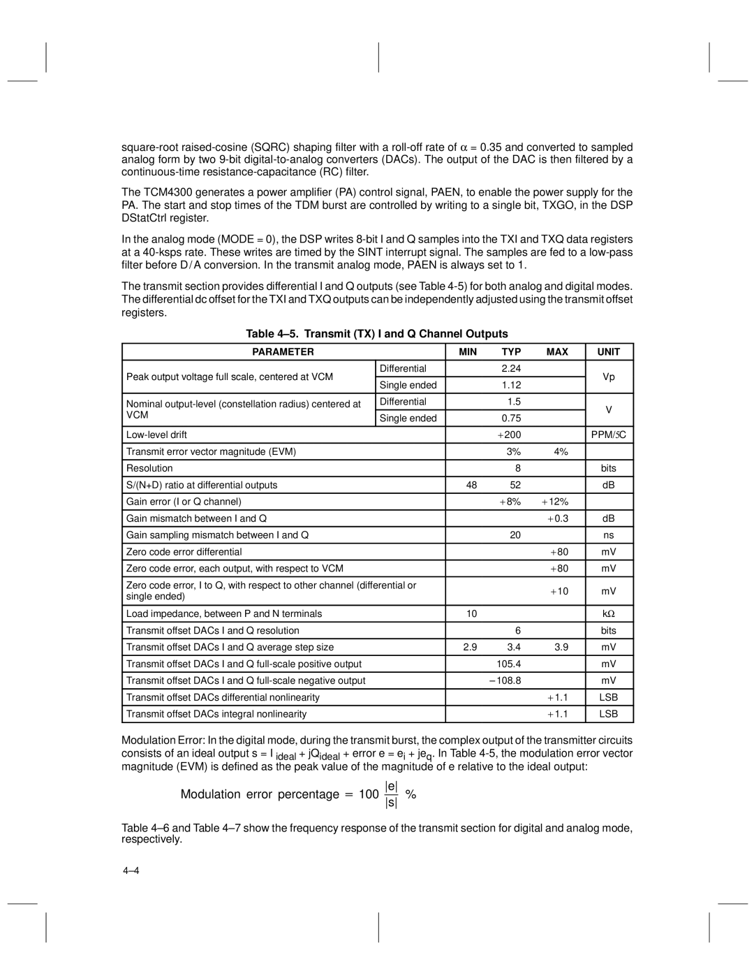
±5. Transmit TX I and Q Channel Outputs
Modulation error percentage +100 s %
Transmit Burst Operation Digital Mode
±6. Transmit TX Channel Frequency Response Digital Mode
±7. Transmit TX Channel Frequency Response Analog Mode
±1. Power Ramp-Up/Ramp-Down TIming Diagram
Wide-Band Data Demodulator
Transmit I And Q Output Level
Parameter Test Conditions MIN MAX Unit Mean CNR
±8. Typical Bit-Error-Rate Performance Wbdbw =
Wide-band Data Interrupts
±9. Bits in Control Register WBDCtrl
WBD
Wide-band Data Demodulator General Information
Auxiliary DACs, LCD Contrast Converter
±10. Auxiliary D/A Converters
±11. Auxiliary D /A Converters Slope AGC, AFC, Pwrcont
±12. Auxiliary D /A Converters Slope Lcdcontr
RSSI, Battery Monitor
±13. RSSI/Battery A/D Converter
Timing And Clock Generation
Sample Interrupt Sint
Clock Generation
Speech-Codec Clock Generation
Microcontroller Clock
Phase-Adjustment Strategy
RCO
Mclkin
Mclken
Frequency Synthesizer Interface
Syndta
Clkpol Numclks Lowval
Highval
MSB/LSB First
Name Description
±14. Synthesizer Control Fields
Synclk Syndta SYNLE1 SYNLE0 Synrdy
Power Control Port
15. External Power Control Signals
Name Suggested External Application Reset
Fmrxen Scen
Iqrxen Txen Mode
WBD Wbdon
OUT1
Cint DSP
Microcontroller-DSP Communications
Dint
Fifo a Fifo B
±16. Microcontroller Register Map
Microcontroller Register Map
Wide-Band Data/Control Register
±17. Microcontroller Register Definitions
Addr Name Category
BIT Name Function Reset Value
Microcontroller Status and Control Registers
±18. WBDCtrl Register
Lcden
LCD Contrast
±19. MStatCtrl Register Bits
LDC D/A
DSP Register Map
±20. DSP Register Map
±21. DSP Register Definitions
DSP Strb INT
Wide-Band Data Registers
Base Station Offset Register
Dspcsl TCM4300 Dsprw Dspstrbl Sint Cint Bdint
±22. DStatCtrl Register Bits
DSP Status and Control Registers
±23. Power-On Reset Register Initialization
Reset
Power-On Reset
Internal Reset State
Microcontroller Interface
Intel Microcontroller Mode Of Operation
±24. Microcontroller Interface Configuration
±25. Microcontroller Interface Connections for Intel Mode
IRQ NMI Dint
Mitsubishi Microcontroller Mode of Operation
Motorola Microcontroller Mode of Operation
Mcrw Mcds
CS3
±32
PZ S-PQFP-G100
Mechanical Data
Important Notice