Agilent Technologies HDMP-3001 manual Internal Functional Blocks, See the block diagram

Models: HDMP-3001

1 124
Download 124 pages 6.83 Kb
Page 5
Image 5

1. Introduction

The Agilent HDMP-3001 is a highly integrated VLSI device that provides mapping of Ethernet en- capsulated packets into STS-3c payloads. The HDMP-3001 sup- ports full-duplex processing of SONET/SDH data streams with full section, line, and path over- head processing. The device supports framing pattern, scrambling/descrambling, alarm signal insertion/detection, and bit interleaved parity (B1/B2/B3) processing. Serial interfaces for SONET/SDH TOH overhead bytes are also provided. The HDMP- 3001 provides a line side interface that operates at 155.52 Mb/s (8-bit bus at 19.44 MHz). For Ethernet applications a system interface operating at 25 MHz is provided. LAPS (Link Access Procedure – SDH) support includes framing, transparency processing, 32-bit FCS processing, and self- synchro- nous scrambling/descrambling (X43 +1). The HDMP-3001 also provides GFP (Generic Framing

Procedure) support which in- cludes framing, 32-bit FCS processing, 16-bit HEC process- ing, and self-synchronous scrambling/descrambling

(X43 +1).

1.1Internal Functional Blocks

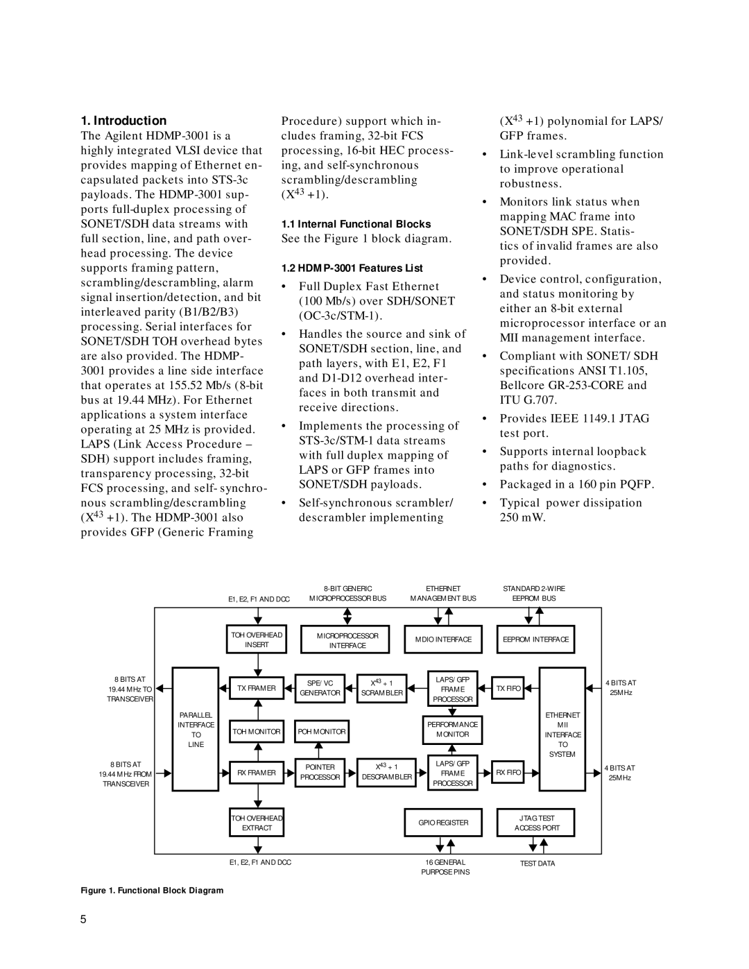
See the Figure 1 block diagram.

1.2HDMP-3001 Features List

Full Duplex Fast Ethernet

(100 Mb/s) over SDH/SONET (OC-3c/STM-1).

Handles the source and sink of SONET/SDH section, line, and path layers, with E1, E2, F1 and D1-D12 overhead inter- faces in both transmit and receive directions.

Implements the processing of STS-3c/STM-1 data streams with full duplex mapping of LAPS or GFP frames into SONET/SDH payloads.

Self-synchronous scrambler/ descrambler implementing

(X43 +1) polynomial for LAPS/ GFP frames.

Link-level scrambling function to improve operational robustness.

Monitors link status when mapping MAC frame into SONET/SDH SPE. Statis- tics of invalid frames are also provided.

Device control, configuration, and status monitoring by either an 8-bit external microprocessor interface or an MII management interface.

Compliant with SONET/ SDH specifications ANSI T1.105, Bellcore GR-253-CORE and ITU G.707.

Provides IEEE 1149.1 JTAG test port.

Supports internal loopback paths for diagnostics.

Packaged in a 160 pin PQFP.

Typical power dissipation 250 mW.


8-BIT GENERIC

ETHERNET

STANDARD 2-WIRE

E1, E2, F1 AND DCC

MICROPROCESSOR BUS

MANAGEMENT BUS

EEPROM BUS


TOH OVERHEAD

MICROPROCESSOR

MDIO INTERFACE

EEPROM INTERFACE


INSERT

INTERFACE


8 BITS AT


TX FRAMER

SPE/VC

X43 + 1

LAPS/GFP

TX FIFO

19.44 MHz TO


GENERATOR

SCRAMBLER

FRAME

TRANSCEIVER


PROCESSOR


PARALLEL


ETHERNET


INTERFACE

TOH MONITOR

POH MONITOR


PERFORMANCE

MII


TO


MONITOR

INTERFACE


LINE


TO


SYSTEM

8 BITS AT


RX FRAMER

POINTER

X43 + 1

LAPS/GFP

RX FIFO

19.44 MHz FROM


PROCESSOR

DESCRAMBLER

FRAME

TRANSCEIVER


PROCESSOR


TOH OVERHEAD


GPIO REGISTER

JTAG TEST


EXTRACT


ACCESS PORT


E1, E2, F1 AND DCC

16 GENERAL

TEST DATA


PURPOSE PINS


4 BITS AT

25MHz

4 BITS AT

25MHz

Figure 1. Functional Block Diagram

5

Page 5
Image 5
Agilent Technologies manual Internal Functional Blocks, See the block diagram, HDMP-3001 Features List

HDMP-3001 specifications

Agilent Technologies, a prominent name in electronics and measurement technology, offers a wide range of products that cater to various industries. Among its notable offerings is the HDMP-3001, a high-speed, serial data transceiver designed to facilitate robust communications in electronic systems. The HDMP-3001 stands out with its ability to handle high bandwidths, making it particularly suited for applications requiring rapid data transfer, such as telecommunications, computer networking, and high-performance computing.

One of the main features of the HDMP-3001 is its advanced signaling technology. By employing differential signaling, the transceiver minimizes electromagnetic interference and enhances signal integrity. This is crucial in environments with multiple electronic devices operating simultaneously, as it ensures data is transmitted clearly and without degradation.

The HDMP-3001 operates at a maximum data rate of 1 Gbps, allowing for efficient data transfer over short distances. This capability is coupled with a flexible architecture that enables users to configure the transceiver for various applications. The device supports both point-to-point and point-to-multipoint configurations, giving engineers the versatility they need in designing communication links.

Moreover, the HDMP-3001 features on-chip clock recovery functionality, which simplifies system design by reducing the number of external components needed. This built-in feature allows the transceiver to maintain synchronization even as data rates increase, further enhancing performance.

The low power consumption characteristic of the HDMP-3001 is another notable advantage. This makes it an attractive choice for battery-operated devices and systems where power efficiency is critical. The transceiver’s design ensures optimal performance while minimizing heat generation and power draw, enabling longer operational lifetimes.

In terms of physical characteristics, the HDMP-3001 comes in a compact, surface-mount package, allowing for easier integration into various circuit board designs. The small form factor, combined with its innovative technology, makes it a popular choice among engineers seeking to improve data transmission reliability without compromising on space or power constraints.

Overall, Agilent Technologies' HDMP-3001 is a formidable solution for high-speed serial data transmission, characterized by its robust performance, low power consumption, and versatile configuration options. With these features, it continues to be an essential component in the evolving landscape of electronic communications.