bmRequest
Field
Description
Vendor Request, IN


Y


R


A


For current information contact Analog Devices at (781) 461-3881


October 2000


N


I


L


M

A


I


C


L


Table 18. USBI

MCUCODE (Code Download) (Continued)


E


N


R


H

A


P


C


E


T Field


Size

Value

Description


Offset


T


A


5


D


wIndex (H)


1

0x00


6


wLength (L)


1

0xXX1

Length = XX bytes


7


wLength (H)


1

0xYY2

Length = YY bytes

1XX is user-specified.

2YY is user-specified.

ADSP-2192

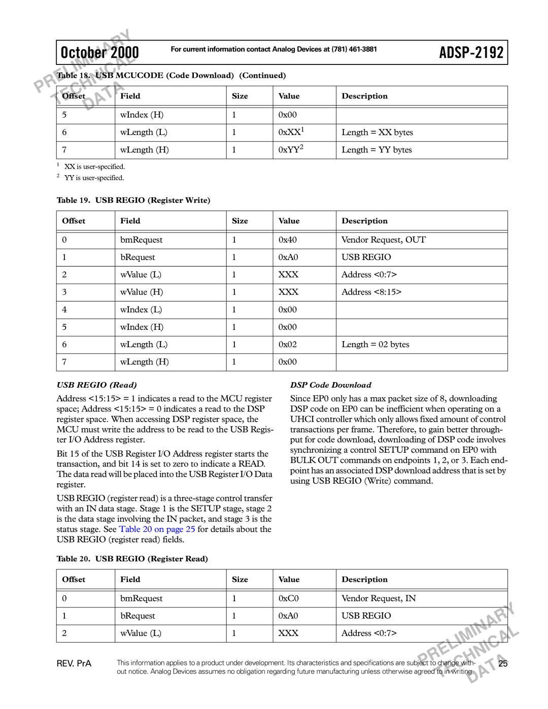
Table 19. USB REGIO (Register Write)

Offset

Field

Size

Value

Description


0

bmRequest

1

0x40

Vendor Request, OUT


1

bRequest

1

0xA0

USB REGIO


2

wValue (L)

1

XXX

Address <0:7>


3

wValue (H)

1

XXX

Address <8:15>


4

wIndex (L)

1

0x00


5

wIndex (H)

1

0x00


6

wLength (L)

1

0x02

Length = 02 bytes


7

wLength (H)

1

0x00


USB REGIO (Read)

Address <15:15> = 1 indicates a read to the MCU register space; Address <15:15> = 0 indicates a read to the DSP register space. When accessing DSP register space, the MCU must write the address to be read to the USB Regis- ter I/O Address register.

Bit 15 of the USB Register I/O Address register starts the transaction, and bit 14 is set to zero to indicate a READ. The data read will be placed into the USB Register I/O Data register.

USB REGIO (register read) is a three-stage control transfer with an IN data stage. Stage 1 is the SETUP stage, stage 2 is the data stage involving the IN packet, and stage 3 is the status stage. See Table 20 on page 25 for details about the USB REGIO (register read) fields.

DSP Code Download

Since EP0 only has a max packet size of 8, downloading DSP code on EP0 can be inefficient when operating on a UHCI controller which only allows fixed amount of control transactions per frame. Therefore, to gain better through- put for code download, downloading of DSP code involves synchronizing a control SETUP command on EP0 with BULK OUT commands on endpoints 1, 2, or 3. Each end- point has an associated DSP download address that is set by using USB REGIO (Write) command.

Table 20. USB REGIO (Register Read)

Offset

Size

Value

0

1

0xC0

1

2

REV. PrA

bRequest

1

0xA0

USB REGIO


Y


R


A

wValue (L)

1

XXX

Address <0:7>


N

L


I


M


A


I


C


L


E


I


N


R


H


This information applies to a product under development. Its characteristics and specifications are subjectPto change with-


A25


C


out notice. Analog Devices assumes no obligation regarding future manufacturing unless otherwise agreed toEin writing.


T

A


T


D


Page 25
Image 25
Analog Devices ADSP-2192 specifications USB Regio, BRequest 0xA0, WValue L, Address

ADSP-2192 specifications

The Analog Devices ADSP-2192 is a high-performance digital signal processor (DSP) that stands out in the realm of signal processing applications. The device is part of the ADSP-2100 family, which has been recognized for its ability to deliver high-speed computations and efficient processing capabilities. The ADSP-2192 is particularly well-suited for applications requiring advanced digital signal processing, such as telecommunications, audio processing, and industrial control systems.

One of the key features of the ADSP-2192 is its dual-core architecture. This allows for parallel processing capabilities, enabling the device to handle multiple tasks simultaneously. Each core can execute instructions independently, which significantly boosts the overall processing power. The device is built on a 16-bit architecture, supporting 16-bit fixed-point and 40-bit floating-point operations, allowing for a wide range of precision in calculations.

The ADSP-2192 also incorporates a sophisticated instruction set designed for efficient performance. It includes specialized instructions tailored for common signal processing tasks, such as filtering and Fourier transforms. This optimized instruction set enhances the speed and efficiency of data manipulation and computation, making it an ideal choice for real-time applications.

In terms of memory, the ADSP-2192 is equipped with 1 KB of on-chip program memory and 2 KB of data memory. This provides sufficient storage for handling complex algorithms without the need for external memory, reducing latency and increasing processing speed. The device also supports external memory interfaces, enabling developers to expand the system's memory capacity if needed.

Another standout feature of the ADSP-2192 is its rich set of communication interfaces. It supports a variety of communication protocols, including SPI, USART, and I2C, facilitating seamless integration with other devices and systems. This versatility makes it suitable for a wide range of applications, from consumer electronics to industrial automation.

In terms of power consumption, the ADSP-2192 is designed to be energy-efficient, making it an excellent choice for battery-operated devices and applications requiring low power usage. The device operates at a voltage range of 3V to 5V, making it compatible with various power supply systems.

Overall, the Analog Devices ADSP-2192 combines powerful processing capabilities with efficient resource management and versatility, making it a strong contender in the DSP market. Its dual-core architecture, robust instruction set, communication flexibility, and energy-efficient design position it as an essential component for advanced signal processing applications across multiple industries.