CHAPTER 2 MEMORY SPACE
2.2.1Data Area
The F2MC-8FX CPU data area can be divided into the following three for each purpose:
•General-purpose register bank area
•Stack area
•Direct area
■General-Purpose Register Bank Area
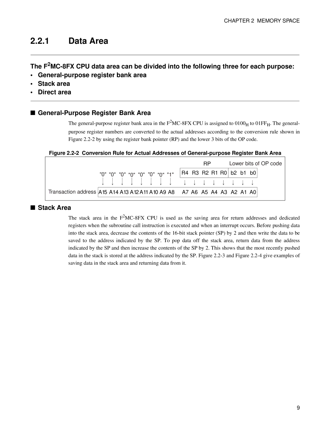
The general-purpose register bank area in the F2MC-8FX CPU is assigned to 0100H to 01FFH. The general- purpose register numbers are converted to the actual addresses according to the conversion rule shown in Figure 2.2-2by using the register bank pointer (RP) and the lower 3 bits of the OP code.
Figure 2.2-2 Conversion Rule for Actual Addresses of General-purpose Register Bank Area
"0" "0" "0" "0" "0" "0" "0" "1"
| RP | Lower bits of OP code |
R4 | R3 R2 R1 R0 | b2 | b1 | b0 | |
| | | | | |
Transaction address A15 A14 A13 A12 A11 A10 A9 A8 A7 A6 A5 A4 A3 A2 A1 A0
■Stack Area
The stack area in the F2MC-8FX CPU is used as the saving area for return addresses and dedicated registers when the subroutine call instruction is executed and when an interrupt occurs. Before pushing data into the stack area, decrease the contents of the 16-bit stack pointer (SP) by 2 and then write the data to be saved to the address indicated by the SP. To pop data off the stack area, return data from the address indicated by the SP and then increase the contents of the SP by 2. This shows that the most recently pushed data in the stack is stored at the address indicated by the SP. Figure 2.2-3and Figure 2.2-4give examples of saving data in the stack area and returning data from it.