Manuals
/
Fujitsu
/
Computer Equipment
/
Computer Drive
Fujitsu
MPA3026AT, MPA3043AT, MPA3052AT, MPA3035AT, MPA3017AT
manual
PR4 signal transfer
Models:
MPA3017AT
MPA3035AT
MPA3026AT
MPA3052AT
MPA3043AT
1
52
176
176
Download
176 pages
49.61 Kb
49
50
51
52
53
54
55
56
Specs
Install
MPA30xxAT Block diagram
PR4 signal transfer
Factory default setting
Dimension
drives configuration
Reset
Diagnostic code
Command block registers
Page 52
Image 52
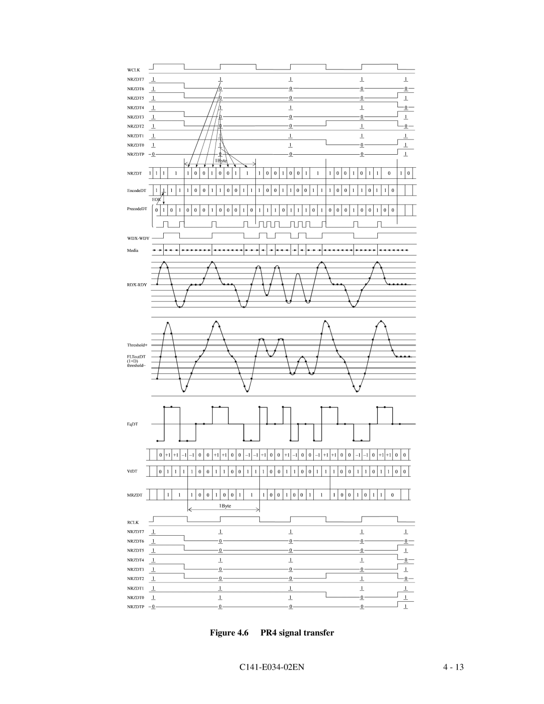
Figure 4.6 PR4 signal transfer
C141-E034-02EN
4 - 13
Page 51
Page 53
Page 52
Image 52
Page 51
Page 53
Contents
C141-E034-02EN
Revision Record
Preface
Chapter
Conventions for Alert Messages
Liability Exception
Contents
Theory of Device Operation
Interface
Operations
Page
Figures
Page
Tables
Features Functions and performance
Device Overview
Adaptability
Interface
Page
Device Specifications Specifications summary
Specifications
Model and product number
Model names and product numbers
Current and power dissipation
Current fluctuation Typ. at +5V when power is turned on
Acoustic noise specification
Shock and vibration specification
MTBF=
Error Rate
Device Configuration System Configuration
Disk drive outerview
Page
Configuration of disk media heads
System Configuration ATA interface
2 1 drive connection
2 drives configuration
3 2 drives connection
Installation Conditions
Dimensions Mounting Cable Connections Jumper Settings
Dimensions
Orientation
Limitation of side-mounting
PCA
Page
Service area
Cable Connections Device connector
Connector locations
Cable connector specifications
Specters Strip
AMP
Device connection
+12V Return +5V Return
Power supply connector CN1
CN1
Factory default setting
11 Factory default setting Jumper configuration
13 Jumper setting of Cable Select
14 Example 1 of Cable Select
092
Outline
Disk
Head
Head structure
Actuator
Spindle
Air filter
Circuit Configuration
MPA30xxAT Block diagram
Power-on Sequence
Power-on operation sequence
Self-calibration contents
Self-calibration execution timechart
Command processing during self-calibration
Write circuit
Read/write preamplifier PreAMP
Write precompensation algorithm
Read/write circuit block diagram
Frequency characteristic of programmable filter
Read circuit
PR4 signal transfer
Time base generator circuit
Write clock frequency and transfer rate of each zone
Servo control circuit
Physical sector servo configuration on disk surface
Page
Servo frame format
Data-surface servo format
PAD
Actuator motor control
Spindle motor control
Page
Chapter Interface
Chip Select RESET- Reset Csel Cable Select GND Ground
Physical Interface Interface signals
Chip Select
Signal assignment on the connector
Signal assignment on the interface connector
Reset
Dasp GND
IOR
Hdmardy
Hstrobe
Pidag
Ddmardy
Iordy
Dstrobe
1 I/O registers
Registers
DA2 DA1 DA0
Command block registers
Icrc UNC Idnf Abrt TK0NF Amnf
Page
DEV HS3 HS2 HS1 HS0
BSY Drdy DSC DRQ Corr ERR
Page
Control block registers
Srst
Command code and parameters
Command code and parameters 1
Command code and parameters 2
Standby Immediate Sleep Check Power Mode Smart
LBA
Command descriptions
LBA LSB
LBA
Read Multiple XC4
Execution example of Read Multiple command
BSY Drdy Intrq DRQ
LBA
LBA
LBA
Write Multiple XC5
LBA
Write Verify X3C
LBA
1F3 HSN Sector No
Initialize Device Parameters
Identify Device XEC
Page
Information to be read by Identify Device command 1
Information to be read by Identify Device command 2
Information to be read by Identify Device command 3
SET Features XEF
Identify Device DMA XEE
‘BB’
Features register values and settable modes
‘CC’
SET Multiple Mode XC6
Page
Diagnostic code
Page
LBA
LBA
Write Buffer XE8
Page
Page
Page
Page
XFF
Page
Features Register values subcommands and functions
’DA’
Page
Format of device attribute value data
1FE 1FF
Format of insurance failure threshold value data
Page
Page
Error posting
10 Command code and parameters
∙ Execute Device Diagnostic ∙ Initialize Device Parameters
Data transferring commands from device to host
BSY Drdy DRQ Intrq
DRQ Intrq
BSY Drdy DRQ Intrq
Write Sectors command protocol
Commands without data transfer
BSY Drdy Intrq
Other commands
DMA data transfer commands
∙ Read Multiple ∙ Sleep ∙ Write Multiple
∙ Read DMA ∙ Write DMA
DRQ Dmarq Dmack
IOW
Ultra DMA feature set Overview
Phases of operation
Pausing an Ultra DMA data in burst
Data in transfer
Terminating an Ultra DMA data in burst
Page
Page
Pausing an Ultra DMA data out burst
Data out transfer
Terminating an Ultra DMA data out burst
Page
Ultra DMA CRC rules
Series termination required for Ultra DMA
11 Recommended series termination for Ultra DMA
DIOR-HDMARDY-HSTROBE
DIOW-STOP
Timing PIO data transfer
DIOR-/DIOW
IOCS16 Iordy
Single word DMA data transfer
Dmarq Dmack DIOR-/DIOW
11 Multiword DMA data transfer timing mode
Multiword data transfer
Ultra DMA data transfer
12 Initiating an Ultra DMA data in burst
Name Mode Comment MIN MAX
Dmardy
Pull-up time before allowing Iordy to be
Sustained Ultra DMA data in burst
13 Sustained Ultra DMA data in burst
Host pausing an Ultra DMA data in burst
14 Host pausing an Ultra DMA data in burst
Device terminating an Ultra DMA data in burst
15 Device terminating an Ultra DMA data in burst
Host terminating an Ultra DMA data in burst
16 Host terminating an Ultra DMA data in burst
17 Initiating an Ultra DMA data out burst
Sustained Ultra DMA data out burst
18 Sustained Ultra DMA data out burst
Device pausing an Ultra DMA data out burst
19 Device pausing an Ultra DMA data out burst
Host terminating an Ultra DMA data out burst
20 Host terminating an Ultra DMA data out burst
21 Device terminating an Ultra DMA data out burst
BSY Dasp
Power-on and reset
BSY Pdiag Dasp
Chapter Operations
Response to power-on
Pdiag Dasp
Response to hardware reset
Response to software reset
Response to diagnostic command
Default parameters
MPA
Logical address
LBA0 LBA1 LBA2
Power save mode
LBA LBA
Page
Power commands
Spare area
Alternating defective sectors
Alternate cylinder assignment
Data buffer configuration
Caching operation
∙ Read Sector S ∙ Read Multiple ∙ Read DMA
∙ Write Sectors ∙ Write DMA ∙ Write Multiple
Usage of read segment
HAP
DAP
Mis-hit data Empty data
Read-ahead data
HAP
HAP set to hit position for data transfer
Partially hit data Lack data
Write Cache
∙ Write Sectors ∙ Write Multiple ∙ Write DMA
Fujitsu Limited FAX
Fujitsu España S.A
Fujitsu Limited
Top
Page
Image
Contents